13 Key Considerations for Aerospace RF/Microwave Devices

This file type includes high resolution graphics and schematics when applicable.

Breakdown Constraints
RF/microwave components in the aerospace channel must be able to withstand extreme conditions, of course, but beyond simply functioning in survival mode, these components must continue to satisfy stringent performance criteria. RF/microwave components tend to be mission-critical. It is therefore necessary to design these components with breakdown constraints in mind.
1. Space-Breakdown Mechanisms. For RF/microwave technology designers who are familiar with space applications, the enormous differences in temperature and pressure are a given. Temperature operation ranges have been designed for, simulated, and predicted with a good level of accuracy. Though they are challenging, it also is possible to account for temperature extremes. Physical stressors, such as vibration, shock, and pressure differentials, are familiar enemies as well. A greater challenge is predicting unique material, radiation, and electrical phenomena, which can lead to component degradation and, later, system failure.
2. Outgassing. Many materials developed in a pressurized atmosphere trap various liquids and gases in their structure. When encountering a high-vacuum environment, these gases and liquids may begin to creep out of the material. Occasionally, this significantly changes the material properties. The level of outgassing exhibited by a material and its effects are difficult to model or simulate. Therefore, NASA has developed a database of materials and their estimated outgassing behavior through batteries of experiments.
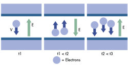
When resonant, these electrons can quickly cascade due to self-amplification. They will then create significant, and potentially damaging, electric discharge. The wall material can be characterized for its potential to induce secondary electron emission yield (SEY), which defines its potential as a space-grade material.
4. Corona. Free electron emissions in space can also wreak havoc when interacting with the ionized atmospheric gas trapped with RF/microwave devices. If the energy of these electrons increases because of a spacecraft’s RF/microwave electronics, the electrons can excite the gaseous molecules within the devices. If the energy of the excitation is high enough, additional electrons may be released. This local electron population growth could exceed the diffusion rate and cause coronal discharge of radiation.
Additionally, the high concentration of electrons could lead to RF reflections—potentially damaging the sensitive RF devices. Increased power density and component integration also make RF/microwave assemblies more susceptible to corona effects.
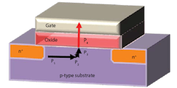
5. Solid-State-Transistor Breakdown Mechanisms. Because many RF parts are now solid-state, these systems are subject to the breakdown mechanisms that are inherent to semiconductor technology. In most aerospace applications, RF/microwave devices need to be rated for survivability under all environmental conditions spanning several years and up to decades. Each solid-state failure mechanism must therefore be identified, designed against, and verified under the strictest standards.
Hydrostatic stress gradients can drive electromigration, thus inducing voids in integrated-circuit (IC) metallization. This stress-induced-voiding (SIV) phenomenon can lead to cracks, fractures, and warping of the metallization layers, corrupting performance. Mechanical stresses, which arise from coefficient-of-thermal-expansion (CTE) mismatches, can add further stress to IC metallization. The result is increased metallization failures.
7. Electromigration. Under high-current conditions, ions within a conductor can gradually travel in response to momentum transfer by electrons and diffusing metal atoms. Higher current density increases the likelihood of electromigration. Like stress migration, electromigration can induce voiding-related failures.
This file type includes high resolution graphics and schematics when applicable.
NBTI, TDDB, and More
This file type includes high resolution graphics and schematics when applicable.
8. Hot Carrier Injection. When an electron or hole gains a sufficient amount of kinetic energy, it may be able to overcome the potential barrier at an interface. If the carrier is injected into the gate dielectric of a metal-oxide-semiconductor field-effect transistor (MOSFET), however, it may become trapped. As a result, the electrical characteristics of the device may be permanently changed. Hot carrier injection (HCI) is one of the most significant limiting factors affecting the reliability of a MOSFET device.
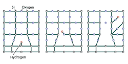
Also affecting MOSFETs, NBTI can lead to transconductance degeneration of the transistor. Over time and under negative voltage-bias conditions, the device’s material property changes can result in increased threshold voltage. Both temporary traps and permanent interface traps can develop in the material, which induces silicon-hydrogen breaks. The migrating hydrogen can later merge with oxygen, leaving dangling silicon bonds and increasing threshold voltage. It is believed that nitrogen—used to retard boron penetration—may be responsible for increased NBTI in both p- and n-type MOSFETs.
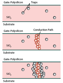
10. Time-Dependent Dielectric Breakdown (TDDB). When a steady voltage is applied across them, many performance dielectric materials experience time-related degradation. TDDB is thought to occur when conductive paths are formed through the gate-oxide substrate as electrons tunnel through the material. Higher densities of electrons tend to accelerate TDDB—an inevitability with MOSFETs. Accelerated statistical testing is used to develop reliability plots to predict TDDB failures.
11. Military & Aerospace Standards. Aerospace organizations have high reliability expectations. Therefore, many standards and qualifying tests have been developed to ensure that only high-reliability parts are used in real systems. These qualifications cover virtually every component of an RF/microwave system with a battery of requirements.
For example, the U.S. Department of Defense has developed a wide range of “mil standards” in order to prevent the inclusion of unqualified parts. Additionally, NASA has performed many qualifying tests in order to recommend parts that are known to have performed well in prior space applications. Yet many part failures still occur, prompting greater investigation into how to effectively analyze and predict breakdowns.

12. Simulating RF Breakdown. Testing for device breakdown vectors traditionally requires huge numbers of tests and many layers of qualifications. Rising costs and shrinking design cycles are hampering the deployment of the most effective technology available in real-world applications. In the hunt for methods to accelerate the analysis and prediction of breakdown mechanisms, designers are increasingly relying on advanced electromagnetic, mechanical, and environmental simulators.
These integrated simulation environments, such as CST Studio Suite and Ansys Multiphysics, have the potential to replicate real-world conditions. In some cases, the simulations can be more illuminating than real-world tests. The simulation environments can include models of different physical interactions to reveal their impact on highly detailed 3D structures. As a result, previously masked internal failure modes may become apparent. Such modes may be hard to detect/analyze in real tests and could reduce the number of tests needed.
For example, a recent application note details the use of CST Studio Suite and Spark3D to predict multipaction and coronal discharge within a 2-pole L-Band filter for space applications. A difference of roughly 25% was determined between the tested and simulated breakdown power levels. As shown, simulation tools may have reached a level of sophistication necessary to reduce the need for costly and time-consuming qualification testing.
13. DARPA IRIS. Even if all the right qualification steps are performed, the industry’s reliance on offshore foundries for IC manufacturing still leaves room for counterfeiting and device performance below expectations. In light of such scenarios, DARPA has begun its Integrated and Reliability of Integrated Circuits (IRIS) initiative. This initiative is designed to develop techniques for determining the exact function and behavior of ICs. Through advanced imaging and the device recognition of complementary-metal-oxide-semiconductor (CMOS) circuits, DARPA hopes to use non-destructive computational methods to determine device connectivity. Beyond device modeling and analysis tools, other aspects of the initiative aim to derive reliability information from a small number of IC tests using unique diagnostic techniques.
The potential breakdown mechanisms in RF/microwave devices are increasing with the adoption of higher-performance criteria and more complex levels of integration. Rigorous qualification processes and testing can hopefully ensure that these complex devices operate reliably. Yet such steps are leading to significant cost and time requirements. In the meantime, counterfeiting and out-of-spec devices are contributing to assembly and system failures.
To combat these challenges, research and design techniques for aerospace devices are steadily being enhanced. For example, integrated simulation environments sporting electrical, thermal, mechanical, and other environmental models are now being leveraged to more rapidly gain insight into device failure modes. Additionally, DARPA and other organizations are actively developing advanced techniques to combat counterfeiting. Their goal is to confirm any component before use to avoid unexpected component-related catastrophes.
Resources
Corona Discharge In Microwave Devices: A Comparison of Ionization Rate Models
NASA Electronics Parts And Packaging Program
Improving Cable Performance in Harsh Environments White Paper
DARPA Integrity And Reliability Of Integrated Circuits (IRIS)
This file type includes high resolution graphics and schematics when applicable.
About the Author
Jean-Jacques DeLisle
Jean-Jacques graduated from the Rochester Institute of Technology, where he completed his Master of Science in Electrical Engineering. In his studies, Jean-Jacques focused on Control Systems Design, Mixed-Signal IC Design, and RF Design. His research focus was in smart-sensor platform design for RF connector applications for the telecommunications industry. During his research, Jean-Jacques developed a passion for the field of RF/microwaves and expanded his knowledge by doing R&D for the telecommunications industry.
