LNA Lowers Noise, Raises OIP3 At 3.5 GHz
Low-noise amplifiers (LNAs) improve the sensitivity of a receiver. When designed for high intercept point, they can also expand its dynamic range. What follows is the design of an LNA with sub-1-dB noise figure at 3.5 GHz and +35 dBm output third-order intercept point, based on a low-cost gallium arsenide (GaAs) enhancement-mode pseudomorphic high-electron-mobility-transistor (ePHEMT) monolithic-microwave-integrated-circuit (MMIC) process.
The sensitivity of a receiver practically hinges on the system noise figure (F), because bandwidth (BW) is predetermined by the parameters set forth in a communications standard:1
Receive sensitivity (dBm) =
-174 + 10log BW (Hz) + the minimum (1)
signal-to-noise ratio (dB) + F
An LNA, as its name implies, improves receiver sensitivity by reducing the system noise figure. The Friss equation shows that the noise figure (F1) of the first receiver stage dominates and subsequent stages (i.e. F2, F3) have progressively smaller impact:
F = F1 + (F2 1)/G1 + (F3 1)/G1G2 + (2)
where Gn = the gain of the nth stage in the receive chain.
In a wireless system, a single antenna may be shared by both the transmitter and receiver through either a frequency-selective diplexer or an RF switch in frequency-division-duplex (FDD) time-division-duplex (TDD) operation, respectively. Additionally, a bandpass filter may be inserted before the LNA to prevent blocking or desensitization by a strong out-of-band interferer. Unfortunately, both the duplexer and the filter, being passive components, have RF losses. As these losses occur before the LNA, they have a large impact on the overall receive sensitivity.2 Therefore, the duplexer's and filter's loss specifications are less critical if there is some design margin in the LNA noise figure.
Besides low noise, other critical LNA parameters are gain and linearity. Wireless infrastructure typically consists of a tower-mounted LNA which connects to a ground-level radio hut via a long cable runconsequently, higher gain is desirable for overcoming the cable losses. Linearity is important because the RF spectrum in the tower vicinity can be very crowded due to site sharing with other wireless transmitters. As a solution, a single-stage GaAs ePHEMT MMIC LNA was developed to meet high-performance and low-cost requirements for 3.5-GHz wireless-infrastructure applications.
Page Title
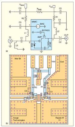
As the block diagram in Fig. 1 shows, the GaAs MMIC consists of a cascode amplifier (AMP) and an active bias regulator (BIAS). The cascode topology was primarily dictated by the requirement for greater than 15 dB small-signal gain at 3.5 GHz, but a previous common-source (CS) design employing the same GaAs ePHEMT process could only achieve about 13 dB gain.3 Although two CS stages can be cascaded to achieve the desired gain, the cascode configuration has the additional advantage of current reusei.e., the same current flows through both stages.
In some receiver implementations, the gain stages following the LNA are bypassed by RF switches when the incoming signals are strong. The change in the LNA load match (GL) due to switching is propagated back to the input match (S11) because the device is non-unilateral (i.e., S12 ≠ 0). Because the antenna and the input filter are very termination-sensitive, they can be detuned by the S11 shift. S11 is less susceptible to load changes when S12 approaches zero, as shown by:
(when S12 → 0)
Since the cascode reverse isolation is 1/200 to 1/2000 that of the CS,4 this is the second reason for choosing the former topology. Direct-conversion receivers, because of their sensitivity to local oscillator self-mixing, also stand to benefit from the enhanced isolation of the cascade configuration.5
Each FET in the cascode received one-half of the total supply voltage, Vdd. As a result, the cascode configuration may have less gain and linearity than the CS configuration under low-voltage operation.6 The ePHEMT technology is ideal for a cascode implementation since it can maintain gain and linearity even when Vds is reduced to 2 V.7 The cascode output is cascaded with a series resistive-capacitive (RC) network to improve the stability above the operating frequency.
3. Simulated stability factor (k) is shown vs. frequency as a function of L2 unloaded Q.
The MMIC is fabricated on a mature and cost-effective 0.25 m process8 that has a gain-bandwidth product, fT, of over 30 GHz. Besides minimizing the number of stages required to achieve the target gain, the high fT also contributes to a low noise figure.9 Additionally, Johnson noise generated in the circuit interconnects is minimized by doubling the metal thickness compared to the previous process amplifier iteration. The 0.64 x 0.64-mm chip fits inside an 8-pin, 2 x 2 x 0.75-mm quad flat no-lead (QFN) plastic package.
The internal bias regulator allows the LNA's quiescent current (Ids) to be controlled through bias resistor RBIAS or an externally applied bias voltage, VBIAS. The regulator's low current drive requirement (IBIAS ≤ 1 mA) is compatible with most CMOS families, and it may be possible to switch the LNA using 5-V logic in TDD applications (switching off the LNA prevents metal migration due to gate current increase during transmit.10,11 The device threshold voltage (VT), forward transconductance (gm), and drain-source resistance, RDS (on) can vary across temperature and between wafers to adversely shift the operating point. Having the bias regulator and LNA on one chip stabilizes the operating point, because VBIAS and VGS voltages will "mirror" each other to compensate for thermal drift12 and gm variations between different wafer batches.
Twelve off-chip components were required for matching, RF decoupling, and biasing, as these functions were not feasible to integrate on the chip. Capacitors C3 and C6 and inductor L1 provide RF decoupling of the gate bias. The C1-L3 L-network transforms active device S11 to Z0 as shown in Fig. 2. The input midband is deliberately offset from perfect match so that it can "wrap around" the center of the Smith chart for wider bandwidth.13 The highpass topology rolls off low-frequency (LF) content, and was chosen due to concern that rising gain below the operating frequency, f0, due to the 6 dB/octave slope, may cause LF instability.
Continue on Page 3
Page Title
The device output impedance, ZOUT, is already close to 50 Ω at f0, so no further matching was necessary. Capacitor C2 and inductor L2 function as a DC block and choke, respectively. They also impart a highpass characteristic to further enhance the LF stability. In the first design iteration, a wire-wound 0402 inductor was used for L2, and this resulted in a Rollett stability factor (k) of 0.94 at the lowest frequency point (11 GHz). When L2 was replaced with a multilayer 0402 inductor in a subsequent prototype, the lowest k marginally improved to 1.2 at 10 GHz (see Fig. 9). It was hypothesized that the multilayer inductor's lower Q at 10 GHz was responsible for the improved stability. The simulated result in Fig. 3 supports the observation that k can be improved by selecting a lower Q in L2. The chip inductors selected for L1 through L3 should have a self-resonant frequency (SRF) above f0. This precaution will ensure the inductors behave predictably at 3.5 GHz.
As the output and input pins are biased from the same voltage supply (Vdd), a portion of the output signals may detrimentally travel back to the input by conduction along the shared DC path. The phasor addition of output and input signals can create gain ripple and even oscillation below f0. To ward off inadvertent output-input feedback over the power supply, decoupling capacitors C3 through C6 shunt the AC signals to ground. Combining small and large capacitances enable suppression over a broader frequency spectrum.
Despite the input match's highpass response, its finite out-of-band rejection permits some leak-through of LF signals. Since the FET gate approximates an open circuit at low frequencies, the signals are then reflected back to the source. As the incidence and reflected input signals vary in phase over frequency, their vectorial addition creates ripples in the input reflection coefficient (ΓIN) as shown in Fig. 4. At the frequencies where the ripple peaks exceed unity, the amplifier is potentially unstable. It follows that the stability criterion k is also less than 1 at the affected frequencies. The countermeasure comprising R2 and C6 reduces ripples below f0 by presenting a resistive termination to reflected signals. RF-grounding capacitor C3 is selected for a reactance (X) of approximately 8 O at f0 so that below 1 GHz, the effects of C3 gradually "disappear." Subsequently, the low frequencies reflected by the gate are diverted to R2 and return to ground through shunt capacitor C6. As the ripples occurred at a frequency interval of about 75 MHz, C6 should be large enough to effectively bypass to this frequency.
To switch the LNA on and off in TDD operation, the Vdd end of RBIAS can be re-connected to 0/5-V control logic. The switching time is constrained by the large time constant of RBIAS and C6 BIAS(C6)>. For a faster turn-on time, C6 can be reduced to the same value as C3. On this evaluation board developed for the LNA, the turn-on time has been measured at approximately 0.6 S using a 10-pF capacitor value for C6.
Continue on Page 4
Page Title
The simplified equivalent circuits of the RLC components were created by intuitively selecting the most important parasitic element, as described by Rhea.16 These component models, which consisted of a two- or three-element equivalent circuit, could only account for the fundamental resonance, whereas real world passives have multiple higher resonances. A more accurate modelling technique such as measurement based models can cover multiple higher resonances,17 but require additional measurements and computer optimization to develop. For designing the LNA impedance-matching network, the simple model's frequency limitation can be tolerated because the main interest is in the frequency range around f0. It is also worth noting that many manufacturer-supplied .s2p files are also frequency limitede.g., most Murata chip capacitors are characterized only to 6 GHz.
The inductor model employed the typical QUL values specified at the frequency nearest to f0 as published in the data sheet (usually 1.7 or 1.8 GHz depending on manufacturer) and then extrapolated to 3.5 GHz and above using a Q proportional to (f)0.5 relationship. An inductor's parasitic capacitance (Cpst) was calculated from the published typical SRF values but with an extra 0.1 pF added to account for the parasitic capacitance associated with the PCB pads. The parasitic inductance (Lpst) in the capacitor model followed the values provided by the vendor-supplied software.18 In the case of L1 and L3, circuit models were subsequently replaced with the manufacturer's .s2p data after the correct inductance value was determined.
5. These diagrams offer a two-level hierarchical model of the level, with (a) the device S-parameter file and input/output matching models, (b) the input equivalent circuit, and (c) the output equivalent circuit.
The evaluation-board printed-circuit board (PCB), which measures 21.5 x 18 mm, uses microstrip transmission lines with a coplanar ground on 10-mil-thick RO4350 laminate material from Rogers Corporation. This mid-priced substrate has modest RF performance and is compatible with FR-4 fabrication processing for ease of producing multilayer designs.14 Since the thin RO4350 PCB is too flexible on its own, an additional 1.2-mm-thick FR-4 layer is glued to the RO4350's ground-plane side for mechanical stability, as well as to make the PCB stack thick enough (1.45 mm) for a snug fit with standard edge-launch RF connectors.
The MMIC's bottom center paddle and pin 4 must be connected to the RF ground using the shortest possible route to minimize deleterious parasitic effects. If significant parasitic inductance exists between the MMIC and the PCB ground plane, gain degeneration and oscillation beyond 10 GHz can occur. In the example layout shown in Fig. 5(b), connection to the bottom ground plane is made using four viaholes that were placed directly under the MMIC. Following good RF practice, all unused MMIC pins (5, 6, and 8) are also connected to ground.
RF connections were made through edge-launch SMA-to-microstrip transitions (Johnson Components part number 142-0701-856), and the DC supply was connected via a two-pin straight PCB header. Other than capacitors C5 and C6, which are 0805 size because of their large values, all other RLC components are 0402 size. The area occupied by components is approximately 8 x 10 mm (see the table for other components). The off-chip circuit was designed by simulation before building the prototype in order to minimize or even eliminate on-the-bench tuning.
To facilitate the design of the matching circuitry, the MMIC's scattering parameters (.s2p file format) were obtained by measuring the physical device on a custom-designed fixture at typical bias conditions. This characterization fixture used the same PCB material (10-mil-thick RO4350 laminate) intended for the prototype LNA. After removing fixture effects from the raw data by the thru-reflect-line (TRL) technique, the resultant .s2p data represented the device and its PCB footprint. The .s2p file was subsequently imported into ADS2006A simulation software from Agilent Technologies for circuit simulation.
During the first simulation iteration, the off-chip components were modelled by employing simplified equivalent circuits. Although manufacturer-supplied .s2p files could be used to model these RLC passive devices, they lacked the convenience of changing component values on the fly and would have slowed down tuning in the simulator. In addition, the .s2p data provided by the capacitor manufacturer is severely limited in usefulness because it has a single reference plane along the chip's long axis15 and hence is only accurate for shunt-connected capacitors. A capacitor in series with the RF path cannot be accurately represented by this data because it is really a two-port device that requires two reference planesi.e., one for each terminal.
Continue on Page 5
Page Title
7. These curves show both measured and simulated noise figure and gain.
The bias section (DC) of the PCB was not modelled because it is not expected to impact the RF performance. The edge-launched SMA jacks (female) were modelled using the ADS2006A parameterized component for a coaxial line with the parameter values from the manufacturer. However, discontinuity effects at the coaxial-to-microstrip interface19 were ignored because additional work would have been required to extract these parameters by either measurement or electromagnetic simulation.
The prototype amplifier was evaluated at room temperature with a supply voltage of 5 V and center frequency of 3.5 GHz. Device current (Idd) was set to 605 mA by using an RBIAS value of 3.3 kΩ. The foremost design goal was to achieve good input return loss (IRL) of better than 15 dB concurrently with low noise figure (less than 1 dB). This requirement originated from the base-transceiver-station (BTS) market segment where the diplexer or filter is termination-sensitive. Older BTS implementations usually rely on either an isolator or a quadrature coupler at the input of the balanced LNA to achieve simultaneous low IRL and noise figure. But newer implementations have sought to eliminate the isolator or the quadrature coupler for both cost and space reasons. In Fig. 6, the measured IRL, output-return-loss (ORL), and isolation (ISO) performance levels at 3.5 GHz were IRL = -16 dB, ORL =-12 dB, and ISO = -32 dB. The IRL minimum occurred about 300 MHz; this was a lower frequency than intended, but no attempt was made to retune the input match because the other requirements had already been met. Besides, it would have required LC values of a finer granularity than the common E12 to shift the mid-band to exactly 3.5 GHz. Immunity to matching components' tolerances should be good, as the bandwidth at the 10-dB RL points was in excess of 1 GHz for both input and output sides. The measured ISO is about 13 dB better than the similar-size single ePHEMT.5 Discrepancies occurred between simulated and measured results, particularly for IRL. This is likely a limitation of the simple PCB models and the passive devices used.
The noise figure was measured at slightly less than 1 dB at 3.5 GHz; the minimum was offset to 3 GHz due to the aforementioned input matching error. The minimum noise figure is about 0.1 dB worse than the reference single PHEMT. Maximum gain of 17.6 dB occurred at 2.6 GHz, but sufficient gain of 15.6 dB is still maintained at the design frequency.
Continue on Page 6
Page Title
The finished LNA was thoroughly investigated for potential instabilities, and the results are graphically portrayed in Fig. 8. Beyond the passband, the gain decreases monotonically with minor inflection points at 14 and 18 GHz. Probable causes of the peaks are component resonances and input-output coupling, but as these peaks are below unity gain, the risk of cavity resonance in an inopportunely-dimensioned metal enclosure is small. The graph also shows the Rollett stability factor, k = (1 + |S11S22-S12S21|2 - |S11|2 - |S22|2)/ (2 |S12S21|) and the stability measure, D = |S11S22-S12S21|; both of these were computed from measured board-level .s2p files. As measurements indicate k > 1 and D 20 Poor agreement between the measured and simulated results above 10 GHz is likely due to model limitations.
Due to receiver component nonlinearities, adjacent-channel signals can create third-order intermodulation distortion (IMD3). The nonlinearity defined by the 2f1-f2 or 2f2-f1 relationship is impossible to filter as they are very close to the desired signal. A key measure of linearity, the third-order intercept point, OIP3, is defined as the point where the fundamental signal power (Pfund) and the IMD3 power theoretically intersect. In the linear region, OIP3 can be calculated from the IMD3 amplitude using Eq. 3:
OIP3 = Pfund + ΔIM/2 (3)
where ΔIM is the difference between the fundamental and the intermodulation product power in dB.
power, third-order intermodulation power,
and IP3 versus frequency.
Two input tones at 3500 and 3501 MHz were used to evaluate the IMD of this design; however, other frequency spacings should not change the results significantly. As shown in Fig. 10, in the linear operating region enclosed by input power (Pi) of less than -4 dBm, the OIP3 is =+35 dBm; this is about 1 dB worse than the single PHEMT, and is remarkable because VDS is one-half the value of the single PHEMT in the cascade configuration. The null, or sweet spot, in the IMD at around -6 dBm input drive is indicative of Class AB operation. The null was caused by the small-signal IMD and large-signal IMD being out-of-phase at the onset of saturation.21
Blocking, which desensitizes the receiver by lowering the gain and increasing the noise figure,22 can be caused by either a nonsynchronous interferer, such as a powerful transmitter sharing the same tower, or by a synchronous source, such as the transmission that leaks past the circulator or duplexer in a transceiver with simultaneous transmit and receive capability.23 A component with a high gain-compression threshold can therefore resist blockers more effectively.
Figure 10 shows an output 1-dB compression point (P1dB) of +19 dBmsimilar to the reference single ePHEMT. Despite the cascode's lower VDS, a high P1dB was obtained because of less heat loss due to the low bulk conductivity of GaAs, as well as the low knee voltage (0.3 V) of the ePHEMT permitting a larger voltage swing before clipping.24 Permitting current Id to follow the square of the RF power (i.e., Id proportional to Po2) like a Class AB power amplifier, also contributes to a higher P1dBa 4-dB improvement at 2.4 GHz has been shown in a similar design.25
In summary, a 3.5-GHz LNA with good noise figure, gain, and linearity was designed around a low-cost, QFN-packaged MMIC. Incorporation of bias regulator, electrostatic-discharge (ESD) protection, and stability network at the chip level reduces the external component count to 12. A proprietary GaAs ePHEMT process from Avago Technologies enabled 15-dB single-stage gain without the usual performance sacrifices, due to cascode transistors operating at one-half VDD.
Acknowledgments
The author would like to thank M.D. Suhaiza and S. Punithevathi for circuit assembly, C.C. Loh for project management, S.A. Asrul for reviewing the article, and the management of Avago Technologies for approving the publication of this work.
References
1. Anonymous, "AN57-1 Fundamentals of RF and Microwave Noise Figure Measurements," Application Note AN57-1, Agilent Technologies, www.agilent.com.
2. I Hunter, R. Ranson, A. Guyette, and A. Abunjaileh, "Microwave Filter Design from a Systems Perspective," IEEE Microwave Magazine, pp. 71-77, Oct. 2007.
3. X. Lu, "Building a 3.3 to 3.8 GHz 802.16a Wimax LNA on FR4 material," Microwave J., Feb. 2006.
4. U.L. Rohde and T.T.N. Bucher, "Chapter 5: Amplifiers and Gain Control" in Communication Receivers: Principles and Design, p. 220, McGraw-Hill Book Co., Singapore, 1994.
5. A.A. Abidi, "Chapter 3: Low Frequency Radio Frequency ICs for Portable Communications" in RF And Microwave Circuit Design for Wireless Communications, L. E. Larson, Ed., Artech House, Norwood, MA, 1997.
6. C. Baringer and C. Hull, "Amplifiers for Wireless Communications" in RF And Microwave Circuit Design for Wireless Communications, L. E. Larson, Ed., Artech House, Norwood, MA, 1997.
7. J. Madden, "Low Voltage Operation of GaAs Power Amplifier," Microwave J., September 2006.
8. K. Fujii and H. Morkner, "Single Supply 1W Ku-band Power Amplifier Based on 0.25gm E-mode PHEMT," Microwave Symposium Digest, 2006.
9. M.F. Danneville, "Microwave Noise and FET Devices," IEEE MW Mag., Oct. 2010, pp. 61-69.
10. Application note No. 1299, "A Low Noise High Intercept Point Amplifier for 900 MHz Applications using the ATF-54143 PHEMT," Avago Technologies, www.avagotech.com.
11. J. Rogers and C. Plett, Radio frequency integrated circuit design, Artech House, Norwood, MA, 2003, "Current Handling in Metal Lines."
12. C. Blair,"Biasing LDMOS FETs for linear operation,"Appl. MW Wireless, Jan. 2000, p. 92.
13. Ray Waugh, "How to design RF circuits for high yields," RF Design, October 2000, pp. 68-72.
14. Product specification "RO4000 Series High Frequency Circuit Materials," rev. 1.4, Available: http://www.rogers-corp.com Rogers Corporation, www.rogerscorp.com.
15. Product specification, "About Characteristic Parameters of Murata Component Library," Murata, www.murata.com.
16. R.W. Rhea, Oscillator Design and Computer Simulation, Noble Pub., Atlanta, 1995, pp. 21-26.
17. Inder Bahl, Lumped Elements for RF and Microwave Circuits, Artech House, Norwood, MA, 2003, Chaps. 2.4.5 and 5.4.4.
18. Murata manufacturing software, "Murata Chip S-Parameter & Impedance Library, V. 3.6.0," 2004.
19. J. Chramiac and J.K. Piotrowski, "Novel approach to the characterization of coaxial-to-microstrip transitions," 27th European Microwave Conference, 1997.
20. Les Besser, "Avoiding RF Oscillation," Applied Microwave & Wireless, Spring 1995, p. 46.
21. P.M. Cabral, J.C. Pedro and N.B. Carvalho, "A Unified Theory for Nonlinear Distortion Characteristics in Different Amplifier Technologies," Microwave Journal, Apr. 2005.
22. W. Domino, N. Vakilian and D. Agahi, "Polynomial Model of Blocker Effects on LNA/Mixer Devices," Applied Microwave & Wireless, Jun. 2001.
23. O. K. Jensen et al., "RF Receiver Requirements for 3G W-CDMA Mobile Equipment," Microwave Journal, pp. 24, Feb. 2000.
24. Der-Woei Wu, J. S. Wei, C. Su, R. M. Parkhurst, SL Fu, S. Chang, and R. B. Levitsky, "An enhancement-mode PHEMT for single-supply power amplifiers," HP Journal, Feb. 1998.
25. Application note, "MGA-634P8 GaAs ePHEMT MMIC 1900 MHz low noise amplifier with superior noise and linearity performance, No. 5475," Avago Technologies, www.avagotech.com.
