Low-Noise Balun Aids Phased-Array Radars
This file type includes high resolution graphics and schematics when applicable.
Active phased-array technology, also known as active electronically scanned array (AESA) technology, has been widely used in commercial, military, and scientific applications.1,2 It supports much faster beam steering than mechanical means, with the capability to prevent interference through the use of strong nulls.3,4
Modern radar systems employ phased arrays that contain thousands of transmit/receive (T/R) modules for electronic beam scanning.2Figure 1 shows a block diagram of a T/R module. The phase shifter is a critical component, used to shift the phase of incoming RF/microwave signals and to meet certain gain, noise, linearity, and phase-shift specifications.
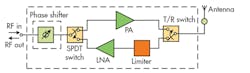
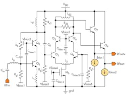
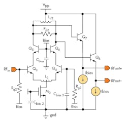
The phase shifter (Fig. 2) is an important part of the T/R module, with a low-noise active balun (LNAB) comprising the first block of the phase shifter following the input signal port. The balun provides impedance matching (at 50 Ω), low-noise amplification, and single-to-differential conversion to provide a quadrature signal to a quadrature-all-pass-filter (QAF) network at X- and Ku-band frequencies. The LNAB circuit is divided into two circuits. The first stage is an active balun which converts single-ended input signals to quadrature signals. Critical performance parameters include high, flat gain, and low noise figure, with good input-output impedance matching.
A number of structures and approaches have been proposed to achieve these goals for the active balun, including a two-stage cascode configuration with passive inductors.7,8 In one of these designs,7 the LNAB provides S21 (gain) of 10 dB, noise figure of 5.4 dB, and power dissipation of 66 mW at 14 to 15 GHz. In the other,8 the simulated S21 performance is 10.2 dB, the noise figure is 4.6 dB, and the power consumption is 87.5 mW at 13 to 15 GHz. Unfortunately, passive inductors contribute to higher loss and larger circuit sizes, and two-stage cascode active baluns have been proposed with active inductors, although these suffered in linearity.4,6 One design offered simulated input third-order intercept point (IIP3) of -30 dBm at 12 GHz. In another design, differential passive inductors were used in an active balun to decrease size and improve circuit performance.9
In pursuit of improved LNAB performance at X/Ku-band frequencies, a two-stage design was developed where the first stage is a single-stage low-noise amplifier (LNA) with cascode configuration. It employs resistive shunt-shunt feedback and peaking inductor for enhanced bandwidth.10,11 The second stage is an active balun with output emitter-follower to convert single-ended input signals to quadrature output signals and provide wideband output impedance matching. The two-stage LNAB was simulated and optimized using the Spectre RF computer-aided-engineering (CAE) software from Cadence Design Systems based on the use of a 0.18-μm silicon-germanium (SiGe) BiCMOS semiconductor technology.
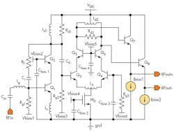
In the proposed LNAB design (Fig. 3), wideband input impedance matching was achieved with a shunt-shunt feedback resistor (Rf) in conjunction with a preceding inductive-capacitive (LC) passive network; flat, high-frequency gain was achieved with the aid of the peaking inductor (Ld1 technique. The second stage is a differential cascode pair with differential peaking inductor (Ld2) to provide the single-ended-to-differential signal conversion, additional common-mode rejection, and wideband output-impedance matching. Use of the differential inductors, Ld2 and L3, save chip space and improve linearity.
This file type includes high resolution graphics and schematics when applicable.
A Closer Look
This file type includes high resolution graphics and schematics when applicable.
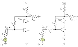
For a better understanding of the resistive shunt-shunt feedback used in the first stage of the LNAB, Fig. 4(a) shows a typical resistive shunt-shunt feedback amplifier. The input impedance, zin and S11 performance of the amplifier can be expressed by Eqs. 1 and 2:
zin = RFB||(1/jwcp, in) = 1/[(1/RFB) + jwcp, in] = 1/yin (1)
|S11| = |(zin – Rs)/(zin + Rs)| = |[(1/Rs) – (1/RFB) – (jwcp, in)]/[(1/Rs) –
(1/RFB) + (jwcp, in)]| (2)
RFB, which is equal to (Rf + Rl′)/(1 – gmlRl′), represents the equivalent resistance looking into the feedback resistor Rf and Rl′ = Rd|| Rl. Parameters cp, in and gml are the parasitic capacitances associated with the input node and the transconductance of the transistor, respectively.
Resistor RFB is often chosen to be equal to Rs, which is the resistance of the voltage source and which is usually 50 Ω for RF systems. At low frequencies, input impedance zin is dominated by RFB. Traditionally, RF is chosen as close to 50 Ω as possible to ensure that the input impedance of the amplifier is well matched before the capacitive effect (jwcp, in) becomes appreciable at higher frequencies. In general, for RF circuits, S11 should be less than -10 dB over the frequency band of interest, as portrayed by Eq. 3:
20log|S11| = 20log[(r – 1)2 + (ωRFBcp, in)2]/[(r + 1)2 + (ωRFBcp, in)2]0.5 ≤ -10 dB (3)
where r = RFB/Rs and the corresponding input-matching bandwidth, f10dB (which equals ω10dB/2π) and the range of r, can be derived by Eq. 4:
f10dB = (-9r2 + 22r - 9r)0.5/(6πRFBcp, in) (4)
From Eq. 4, it can be seen that the input matching bandwidth is directly affected by r, so a suitable value of r was chosen to determine the bandwidth of the LNA.
Figure 4(b) shows the resistive shunt-shunt feedback amplifier with wideband input-impedance matching network and emitter degeneration inductor. The input impedance is given by Eq. 5:
Zin = {(1 + scp, inRFB)[ scp, in(Lg + Ls) + gmLs] + RFB cp, in}/[(1 + scp, inRFB) cp, in] (5)
Assuming that RFB = Z0, frequencies corresponding to Zin = Z0—i. e., a virtually perfect input impedance match—can be derived from Eq. 6:
s2cp, inRFB(Lg + Ls + scp, in(Lg + Ls + RFBgmLs - cp, inRFB2) + gmLs = 0 (6)
There are two frequencies at which a perfect match can be obtained, and the two frequencies are directly affected by shunt-shunt resistor Rf, emitter degeneration inductor, Ls, and base input inductor, Lg. For wideband input impedance matching (S11 < -10 dB) for X- and Ku-band frequencies, the active device (Q1) emitter area is 0.15 × 20 μm, and values for Rf = 950 Ω, Ls = 0.091 nH, and Lg = 0.17 nH were chosen. These component choices set the two pole frequencies at 6.95 and 14.87 GHz, respectively.
The shunt peaking inductor architecture represents an effective methods for improving high frequency gain flatness. It can compensate for decreasing gain with increasing frequency, to achieve flat gain with frequency. The peaking inductor technique also helps reduce the noise figure as well. To analysis the effect of the shunt peaking inductor on gain, Figs. 5(a) and (b) depict a typical resistive shunt-shunt feedback amplifier with peaking inductor and its small-signal equivalent circuit, respectively. From Fig. 5(b), the small-signal gain can be expressed as Eq. 7:
AV = s(Vout/Vin) = [(Rf – gm)RRf2]/[Rf(1 + Rsscp, in + Rs]
[Rf(1 + Rsccs) + R] - RRsRf(Rf – gm (7)
where
R = Rd||SLd and as the frequency increases, the value of SLd increases, making R increase. Increasing R improves the high-frequency gain to help achieve flat gain.11 To achieve adequate gain, a +3.3-VDC supply provides 3.03 mA current, using an emitter area of 0.15 × 20 μm. Shunt peaking, which also helps flatten the gain response, relies on Rd and Ld. For gain flatness with less than 1-dB deviation, values of 650 Ω for Rd and 0.157 nH for Ld were chosen.
This file type includes high resolution graphics and schematics when applicable.
Tracking Noise
This file type includes high resolution graphics and schematics when applicable.
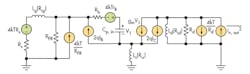
Figure 6 shows the small-signal model of a purely resistive-feedback LNA including all significant sources of noise. Noise contributions from rb are included, but the effects of rb are excluded from the impedance calculations to reduce complexity. The use of emitter degeneration inductor Ls to replace the degenerative resistor can reduce the noise figure effectively, and the shunt peaking inductor Ld can also suppress noise generation.
From Fig. 6, the equivalent input referred noise can be expressed as Eq. 8:
v2n, in/Δf = 4kT(Rs + Rlg + rb + [(4kT/RFB) + 2qIB • (Rs||RFB + Rlg) + 2qIBRls2 + (4kT/(Rd||Rld) + 2qIC)/gm′2| 1 + jω(Rs||RFB + Rlg)c′p, in2| (8)
where Rlg, Rls, and Rld are the equivalent parasitic resistances of inductors Lg, Ls, and Ld, respectively. Also, g′m= gm/(1 + gmRls) and c′p, in = cp, in/(1 + gmRls. From Eq. 8, the value of Rls is the quantity 2qIBRls2 is much less than the value of a standard resistor, so the noise figure is effectively reduced by emitter degeneration inductor Ls.
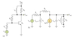
The second stage of the LNAB is the active balun architecture, which converts single-ended input signals to differential output signals. Those signals drive the QAF network, so that good (50 Ω) matching is essential at the output port. Figure 7 shows the schematic diagram of the active balun stage. It is comprised of a differential cascode configuration with output emitter-follower pairs. For good impedance matching of the differential cascode pairs and good current density, the same emitter area of devices Q3 through Q6 was chosen for this, with area of 0.15 × 20 μm. The active balun has total current consumption of 9.37 mA from a +3.3-VDC supply.
The tail current of the differential cascode pairs is generated by m0 with a W/L ratio of 57.3/0.18 μm. Differential inductor L3 is used as an emitter degeneration inductor of the differential cascode pair to improve LNAB linearity and reduce passive inductance and chip size. The value of L3 is chosen at 0.11 nH in an effort to maintain gain. The output load of the active balun is a differential inductor, Ld2, which helped reduce chip area, and resistor, Rd2. For good height and gain flatness, values of 0.495 nH for d2 and 1.08 kΩ for Rd2 were chosen. Good wideband output impedance matching to 50 Ω was achieved by using the output emitter-follower pairs with the tail current of 660 μA. An emitter region area equivalent to that of Q7 – Q8 was used, of 0.15 × 4.8 μm.
The LNAB was simulated and optimized using the Spectre RF computer-aided-engineering (CAE) software from Cadence Design Systems based on a 0.18-μm SiGe BiCMOS technology. Impedance matching in the first stage was achieved by shunt-shunt feedback resistor in conjunction with the LC passive matching network. Component values for the shunt-shunt resistor Rf and inductors Lg and Ls in the LC passive network were adjusted with the help of a Smith chart and parameter sweeping tools. A wideband range of input impedance-matching values with two poles (6.95 and 14.87 GHz) was realized for X- and Ku-band frequencies, with input reflection coefficient of better than -10 dB.
In the second stage of the LNAB, the same emitter region area of devices Q7 and Q8 was chosen to ensure good impedance matching of the differential configuration. The values of differential inductor Ld2 and load resistor Rd2 were adjusted for flat gain, low noise figure, and small chip area. The small chip size and good linearity were also achieved by adjusting the value of differential emitter degeneration inductor (L3) and the length-to-width ratio of the MOS (M0). Finally, the wideband output impedance-matching was achieved by the emitter-follower pair, and choosing a suitable emitting region area of Q7 and Q8 to make sure that the output reflection coefficient is less than -10 dB at X/Ku-band frequencies.
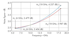
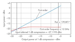
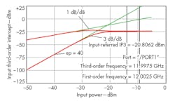
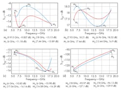
Simulated results of S-parameters, noise figure, output power at 1-dB compression (P1dB), and input third-order intercept point (IIP3) for the LNAB are shown in Figs. 9 through 12. The solid line and dotted line in Figs. 9 and 10 are for simulations without and with parasitic extraction, respectively. Figure 9(a) shows simulated S11 without parasitic extraction, which is better than -10 dB across the full bandwidth. Post-simulation S11 is less than -9 dB from 8.04 to 12.5 GHz. The good S11 performance can be linked to the resistive shunt feedback in conjunction with the LC passive matching network.
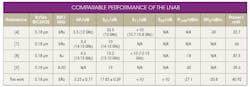
The measured and simulated data are generally consistent for the LNAB. Pre-simulation of S21 revealed 17.83 ± 0.39 dB over X/Ku-band frequencies. Post-simulation of S21 ranges from 16.90 to 18.52 [Fig. 9(b)]. The LNAB’s S22 characteristics are all better than -10 dB, while S12, at better than -90 dB, shows the good isolation achieved in the design. As the table shows, the performance of the LNAB compares favorably with performance levels cited in recent work.4, 7-9
Wang Wei, Professor
Zhong Wu, Engineer
Xu Wei, Engineer
Mu Mao, Engineer
Yuan Jun, Lecturer
College of Electronics Engineering, Chongqing University of Posts and Telecommunications, Chongqing 400065, People's Republic of China.
This file type includes high resolution graphics and schematics when applicable.
References
This file type includes high resolution graphics and schematics when applicable.
1. B.C. Kane, L.A. Geis, M.A. Wyatt, D.G. Copeland, and J.A. Mogensen, “Smart phased array SoCs: A novel application for advanced SiGe HBT BiCMOS technology,” Proceedings of the IEEE, 2005, Vol. 93, No. 9, pp. 1656-1668.
2. T. Dinc, S.I. Zihir, and Y. Kalyoncu, et al., “High performance, SiGe-heterojunction bipolar transistors-low noise amplifier for phased array radar applications,” IET Microwaves, Antennas & Propagation, Vol. 6, No.7, August 11, 2011, pp, 768-772.
3. D. Parker and D.Z. Zimmermann, “Phased arrays–part 1: Theory and architectures,” IEEE Transactions on Microwave Theory & Techniques, Vol. 50, No. 3, March 2002, pp. 678-687.
4. Kwang-Jin Koh and Gabriel M. Rebeiz, “An X- and Ku-Band 8-Element Phased-Array Receiver in 0.18-μm SiGe BiCMOS Technology,” IEEE Solid-State Circuits, Vol. 43, No. 6, June 2008, pp. 1360-1371.
5. Kwang-Jin Koh and G.M. Rebeiz, “A 6-18 GHz 5-Bit Active Phase Shifter,” IEEE Microwave Theory & Techniques Symposium (MTT-S), Technical Digest, 2010, pp. 792-795.
6. Kwang-Jin Koh and G.M. Rebeiz, “An X- and Ku-Band 8-Element Linear Phased Array Receiver,” IEEE CICC, 2007, pp. 761-761.
7. Dong-Woo Kang, G.M. Rebeiz, and Kwang-Jin Koh, “X/Ku-Band SiGe BiCMOS Phased Array Chips with Simultaneous 2- and 4-Beam Capabilities,” IEEE CISC 2009, pp. 1-4.
8. Dong-Woo Kang, Kwang-Jin Koh, and G.M. Rebeiz, “A Ku-Band Two-Antenna Four-Simultaneous Beams SiGe BiCMOS Phased Array Receiver,” IEEE Transactions on Microwave Theory & Techniques, Vol. 58, No. 4, April 2010, pp. 771-780.
9. Yusuf A. Atesal, Berke Cetinoneri, and Kevin M. Ho et al., “A Two-Channel 8–20-GHz SiGe BiCMOS Receiver With Selectable IFs for Multibeam Phased-Array Digital Beamforming Applications,” IEEE Transactions on Microwave Theory & Techniques, Vol. 59, No. 3, March 2011, pp. 716-726.
10. S. Smith, Microelectronic Circuits, 5th ed., Oxford University Press, Oxford, UK, 2004, pp. 818-830.
11. Hsien-Ku Chen and Yo-Sheng Lin, “Analysis and Design of a 1.6-28-GHz Compact Wideband LNA in 90-nm CMOS Using a π-Match Input Network,” IEEE Transactions on Microwave Theory & Techniques, Vol. 58, No. 9, August 2010, pp. 2092-2104.
12. Prabir K. Saha, Subramaniam Shankar, Rob Schmid, and John D. Cresster, “Analysis and Design of a 3-26 GHz Low-Noise Amplifier in SiGe HBT Technology,” IEEE Radio and Wireless Symposium (RWS), 2012.
This file type includes high resolution graphics and schematics when applicable.
