Low-Power UWB CMOS LNA Gains 4 to 5 GHz
This file type includes high resolution graphics and schematics when applicable.
Ultrawideband (UWB) communications offers a great deal of flexibility and versatility for modern users, but it requires advanced analog signal processing, including wideband amplifiers. To meet the growing needs for UWB applications, a low-noise amplifier (LNA) for low-voltage, low-power use was designed for fabrication using 0.18-μm silicon CMOS technology developed by Taiwan Semiconductor Manufacturing Corp. (TSMC).
The LNA operates in the 4- to 5-GHz range and meets the Chinese specifications for UWB systems targeting broadband input matching. In addition, a transconductance (gm) boosting technique helps improve the gain and noise-figure performance levels. Needing less than 0.9-mW total power consumption, the LNA features a low supply voltage of +0.6 V dc.
Since 2002, the Federal Communications Commission (FCC) has authorized UWB systems for use from 3.1 to 10.6 GHz in the United States. The technology offers high data rates at low power levels. In December 2008, the Ministry of Industry and Information Technology (MITT) in China allocated the 4.2- to 4.8-GHz frequency band for UWB applications in that country.1
LNAs—crucial building blocks for wireless receiver front ends—must meet several requirements for practical use. As the first component following an antenna, an LNA must provide full bandwidth impedance matching with low noise figure, sufficient power gain. and acceptable gain flatness. In addition, many wireless UWB applications require low-voltage operation with low power consumption to extend operation under battery power.
LNA Types
A number of CMOS LNAs have been developed for UWB receiver systems.2-9 A conventional distributed amplifier (DA),10-12 for instance, absorbs the parasitic capacitance of the input transistor as part of the transmission line, and thus delivers good wide-frequency performance. However, these amplifiers are rather large in size with relatively high power consumption, making them of limited interest for low-power applications. There’s also the resistive feedback topology,13-15 which provides broadband matching with level gain over wide bandwidths. But it’s still difficult to satisfy high-gain and low-noise-figure requirements simultaneously with this approach.
Amplifier designs have employed passive filtering for extended bandwidths.16-19 By adding a passive inductive-capacitive (LC) network to a conventional cascode structure, a narrowband LNA can be extended to an UWB LNA with good performance in power gain, input matching, and noise figure. But stacking MOS transistors increases the voltage requirements, which more or less negates this approach. On top of that, additional inductors in the LC filter consume physical area and lead to higher costs.
Due to its simplicity, the common-gate (CG) amplifier has become a somewhat popular wideband-amplifier topology.20,21 Proper transconductance of the input transistor achieves wideband matching and high gain. However, parasitic capacitance in this approach could significantly deteriorate noise figure and gain. A gm-boosting technique22,23 can overcome these limitations, although the additional gm stage also leads to higher power dissipation.24
New UWB LNA Approach Gets a Boost
The latest design concept used to conquer the limitations of these LNA design approaches for UWB leverages a novel current-reuse gm-boosted structure. The CG amplifier design employs a common-source (CS) stage to achieve the gm boost; this stage shares bias current with the LNA’s CG stage. Incorporating a forward body bias technique effectively reduces the operating voltage of this LNA. As a result, the LNA design achieves excellent electrical performance at reduced supply voltage and power dissipation, suiting it for low-voltage Chinese UWB applications.
With the current-reuse CG configuration, this new LNA is able to meet impedance-matching requirements for UWB applications, whereas a CS LNA configuration needs additional techniques (and larger circuit size) to fulfill UWB matching requirements. The CG LNA features a simple and robust matching architecture, with good linearity and low power consumption. Because the voltage gain of a CG LNA approach is generally inferior to that of a CS LNA, it uses a gm-boosting technique.
A CG amplifier’s noise performance also comes up short versus that of a CS design. Once again, the gm-boosting approach can be used, this time to help the noise figure. Neglecting induced gate noise, the noise factor of a basic CG LNA has a minimum NF26 according to Eq. 1:
F = 1 + γ/α (1)
where α and γ are bias-dependent parameters.
It’s usually difficult to achieve a noise figure of under 3 dB with a CG LNA approach, and the noise performance typically deteriorates at higher frequencies. A CG LNA also requires an input transconductance of 20 mS for input matching at 50 Ω, which translates into high power consumption. By boosting the transductance, improvements can be made in the CG LNA design.
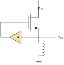
Figure 1 illustrates a gm-boosting approach, where an inverting replica signal with an amplitude n is provided from the source to the gate terminal. Consequently, it boosts the effective transconductance by a factor of (1 + n):
gm, eff = (1 + n)gm (2)
The noise factor (F) becomes:
F = 1 + (γ/α)[1/(1 + n)]|(1 + n)gm R = 1 (3)
A number of gm-boosting methods are presented in the technical literature, either by using active circuitry or passive transformers. For example, a capacitive cross-coupling technique28 can boost transconductance by a factor of 2. But the need for a differential architecture makes this configuration somewhat complex with increased power consumption. A transformer-based approach22,26 is easy to implement, but doesn’t suit UWB applications due to process nonlinearities. Moreover, the parasitic resistance of the inductors can degrade the noise-figure performance.
A gm-boosting CG UWB LNA approach was unveiled in refs. 22 and 27, with a CS stage to provide inverting gm-boosting gain. This active amplifier approach28 provides larger inverted amplitudes than other methods. But the CG stage and the gm-boosting circuits are biased separately using different dc voltage paths, which increases total power dissipation compared to simpler biasing methods.
To minimize power dissipation in the proposed UWB LNA design, a current-reuse architecture is used with the CG stage and gm-boosting circuit stacked together. Sharing current between the gm-boosting stage and the CG stage minimized dc consumption. In addition, a forward body bias technique29 was adopted to relieve the high-voltage supply caused by the stacked structure.
This file type includes high resolution graphics and schematics when applicable.
Forward Body Bias
This file type includes high resolution graphics and schematics when applicable.
Technologically, the most efficient way to reduce amplifier power consumption is through supply voltage scaling. However, a cascade arrangement’s performance will degrade as the supply voltage decreases. For the proposed LNA design, which has two MOSFETs stacked in the first stage, a low supply voltage is impractical. At a supply voltage of +1 V dc, the NMOS transistors still operate in a weak inversion region, which will lead to increased noise figure.
To solve this problem, a forward body bias technique was applied to minimize the threshold voltage, Vth. In a standard silicon CMOS process, the dc bias at the body terminal can manipulate the threshold voltage, adding one more degree of freedom to a circuit design. Typically, the threshold voltage of an n-channel MOSFET is given by Eq. 4:
Vth = Vh 0 + γ[(φf - Vbs)0.5] - (2φf)0.5 (4)
Thus, the source-to-body voltage Vbs can manipulate the threshold voltage (Vth). Voltage Vth 0 is the threshold voltage when Vbs = 0, γ = the bulk threshold parameter, and φf is a semiconductor parameter with a typical value in the range of 0.3 to 0.4 V.29 With the forward body bias technique, the MOSFETs can operate at a reduced bias voltage while still maintaining acceptable gain, linearity, and noise-figure levels.
Two-Stage Architecture
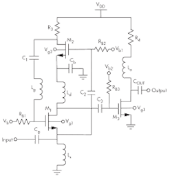
The proposed low-power LNA adopted a two-stage architecture (Fig. 2). The first stage is a CG stage with low input impedance and broadband characteristics, with noise figure almost independent of frequency of operation. The CG stage also eliminates the Miller effect and provides high isolation from output return signals. The gm-boosting inverting stage, CS NMOS amplifier M2, overcomes the inherent low transconductance of the CG LNA, thus improving gain and noise figure as in Eqs. 2 and 3. To minimize current dissipation, the CG LNA and gm-boosting stages are biased using the same dc path, which helps achieve good input matching and noise performance without increasing device size or power dissipation. To boost gain, the CS active device, M3, is designed into the second stage.
At the input stage, gate capacitor Cg and source inductor Ls are part of the matching network to match the input port to 50 Ω. The series-resonant LC tank with gate inductor Lg and capacitor C1 provide low-impedance ac coupling paths between the drain of M2 and the gate of M1. Capacitor Cb is a bypass capacitor that makes high-frequency ac current flow to ground, avoiding signal interference coupling back to M1. Drain inductor Ld acts as an RF choke to isolate devices M1 and M2. The input RF signal is simultaneously fed to the source of M1 and the gate of M2 for amplification; with one path through M2, an inverting signal is applied back to the gate of M1. This increases the equivalent transconductance (gm, eff) of M1, leading to a reduction in the CG LNA’s noise figure.
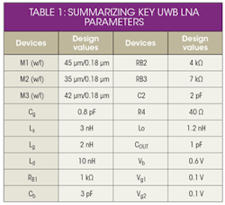
To ensure sufficient gain across the full frequency range, the CS amplifier is used in the second stage. A shunt peaking inductor (L0) and resistor R4 are used to achieve an extension of LNA bandwidth. Table 1 summarizes the design parameters for most instances of the devices in Fig. 2.
Simulation Results
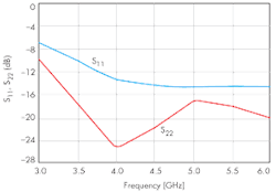
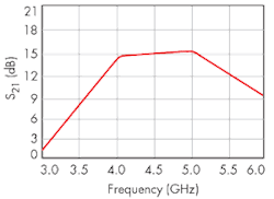
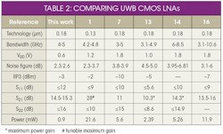
Figure 3 shows the simulated input reflection coefficient S11 and output reflection coefficient S22, which are below -12 and -16 dB, respectively, indicating good impedance matching. Figure 4 shows the LNA’s forward transmission, S21, which ranges from 14.5 to 15.3 dB with gain variations as small as 0.8 dB.
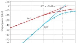
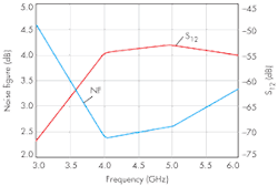
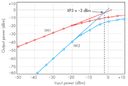
The amplifier design achieves good reverse isolation, with S12 of better than -50 dB, and the simulated noise figure ranges from 2.3 to 2.6 across the frequency range (Fig. 5). The linearity is also acceptable (Fig. 6), with input third-order-intercept point (IIP3) of -3 dBm at 4.5 GHz. The total power dissipation for the LNA design is 0.9 mW from a +0.6-V dc supply.
Acknowledgment
The authors would like to thank the Open Fund Project of Hunan University’s Key Laboratory (Project No.12K012).
Chunhua Wang, Professor
School of Computer and Communication,
Hunan University, Changsha, People’s Republic of China
Wen Wang, Postgraduate Student
College of Information Science and Engineering
Hunan University, Changsha, People’s Republic of China
This file type includes high resolution graphics and schematics when applicable.
References
This file type includes high resolution graphics and schematics when applicable.
1. Fei-hua Chen, Shui-yang Lin, Ling-yun Li, and Xiao-Wei Sun, “4.2-4.8 GHz CMOS Variable Gain LNA for Chinese UWB Application,” International Conference on Microwave and Millimeter Wave Technology, 2010, pp.1922-1924.
2. Ro-Min Weng, Chun-Yu Liu, and Po-Cheng Lin, “A Low-Power Full-Band Low-Noise Ampliï¬er for Ultra-Wideband Receivers,” IEEE Transactions on Microwave Theory and Techniques, 2010, pp. 2077-2083.
3. Chen-Ming Li, Ming-Tsung Li, Kuang-Chi He, and Jenn-Hwan Tarng, “A Low-Power Self-Forward-Body-Bias CMOS LNA for 3–6.5-GHz UWB Receivers,” IEEE Microwave and Wireless Components Letters, 2010, pp. 100-102.
4. Alireza Dehqan, Ehsan Kargaran, Khalil Mafinezhad, and Hooman Nabovati, “An Ultra Low Voltage Ultra Low Power CMOS UWB LNA Using Forward Body Biasing,” IEEE International Midwest Symposium on Circuits and Systems, 2012, pp. 266-269.
5. Giuseppina Sapone and Giuseppe Palmisano, “A 3–10-GHz Low-Power CMOS Low-Noise Ampliï¬er for Ultra-Wideband Communication,” IEEE Transactions on Microwave Theory and Techniques, 2011, pp. 678-686.
6. Yanjie Wang and K. Iniewski, “A Low Power CMOS Low Noise Amplifier for 3-l0 GHz Ultra-wideband Wireless Receivers,” IEEE International Midwest Symposium on Circuits and Systems, 2006, pp. 353-357.
7. Liu Jinhua, Chen Guican, and Zhang Hong, “A 3-5-GHz gm-Boosted Common-Gate CMOS UWB LNA with a Common-Source Auxiliary Circuit,” International Conference on Microwave and Millimeter Wave Technology (ICMMT), 2008, pp. 1342-1345.
8. Bo-Yang Chang and C. F. Jou, “Design of a 3.1-10.6-GHz Low-Voltage, Low-Power CMOS Low-Noise Amplifier for Ultra-wideband Receivers,” Asia-Microwave Conference Proceedings, 2005.
9. Zhe-Yang Huang, Che-Cheng Huang, Chun-Chieh Chen, and Chung-Chih Hung, “A 1-V, 2.39-mW Capacitor-coupling Resonated Low Noise Amplifier for 3-5-GHz Ultra-Wideband System,” IEEE International SOC Conference, 2007, pp. 101-104.
10. Yueh-Hua Yu, Emery Chen, and Deukhyoun Heo, “A 0.6-V Low Power UWB CMOS LNA,” IEEE Microwave and Wireless Components Letters, 2007, pp. 299-231.
11. Brian M. Ballweber, Ravi Gupta, and David J. Allstot, “A Fully Integrated 0.5–5.5-GHz CMOS Distributed Amplifier,” IEEE Journal of Solid-State Circuits, 2000, pp. 231-239.
12. Yueh-Hua Yu, Yi-Jan Emery Chen, and Deukhyoun Heo, “An Ultra-low Voltage UWB CMOS Low Noise Amplifier,” Asia-Pacific Microwave Conference, Yokohama, Japan, 2006, pp.313-316,2006.
13. Zhe-Yang Huang, Che-Cheng Huang, and Chun-Chieh Chen, “A CMOS Low-Noise Amplifier with Impedance Feedback for Ultra-Wideband Wireless Receiver System,” IEEE International Symposium on VLSI Design, Automation, and Test, 2008, pp. 51-54.
14. A. Djugova, J. Radic, and M. Videnovic-Misic, “A 0.18-μm CMOS Low Power LNA for 6–8.5 GHz UWB Receivers,” International Semiconductor Conference, 2011, pp. 215-218.
15. Chang-Wan Kim, Min-Suk Kang, and Phan Tuan Anh, “An Ultra-Wideband CMOS Low Noise Ampliï¬er for 3–5-GHz UWB System,” IEEE Journal of Solid-State Circuits, 2005, pp. 544-547.
16. Yi-Jing Lin, S. S. H. Hsu, Jun-De Jin, and C. Y. Chan, “A 3.1–10.6 GHz Ultra-Wideband CMOS Low Noise Ampliï¬er With Current-Reused Technique,” IEEE Microwave and Wireless Components Letters, 2007, pp. 232-234.
This file type includes high resolution graphics and schematics when applicable.
