This file type includes high resolution graphics and schematics when applicable.
High-frequency switches fabricated with microelectromechanical-systems (MEMS) technology can provide numerous benefits compared to conventional semiconductor switches. These include better amplitude-with-frequency characteristics, lower power consumption, and higher linearity.1 These characteristics make MEMS switches suitable candidates for millimeter-wave applications, provided that adequate isolation and low insertion loss are possible at those higher frequencies. As a result, a number of studies have explored the development of switches for higher-frequency bands, including compact MEMS switches.2,3
MEMS switches are usually divided into contact-type and capacitive-type switches. Contact switches typically have lower insertion losses than capacitive switches over a broad frequency ranges. However, their isolation tends to degrade at higher frequencies, owing to coupling between the open signal and the contact element beyond the desired signal. To examine the possibility of using MEMS technology for a higher-frequency switch, a lateral-contact series MEMS switch was designed for applications from 30 to 40 GHz and simulated by means of commercial computer-aided-engineering (CAE) software. Simulated results indicate low insertion loss of 0.17 dB and high isolation of 36.7 dB (both at 35 GHz), with analysis indicating that insertion loss of less than 0.2 dB and isolation of more than 37.5 dB can be achieved from 30 to 40 GHz.
Normally, the isolation of contact switches is determined by the initial capacitance between the contact metal and the coplanar-waveguide (CPW) transmission line, which is the capacitance between the input and output signal lines. In addition, the coupling capacitance between the input and output ports through the substrate on which the switch is mounted cannot be ignored. To increase the isolation of an RF MEMS switch, the coupling capacitance must be sufficiently minimized. Traditionally, switch coupling capacitance could be minimized by enlarging the gap between the signal lines of the CPW line and the contact element. Unfortunately, this further increases the driving voltage.
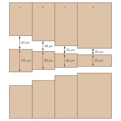
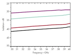
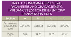
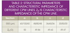
To overcome this tradeoff, a new method was employed by scaling the CPW lines of the switch to achieve higher isolation. Figure 1 shows a schematic view of dCPW transmission lines with different dimensions. The impedances of these CPW lines were calculated with the aid of the Advanced Design System (ADS) CAE software from Agilent Technologies; simulations were performed with the High-Frequency Simulation Software (HFSS) electromagnetic (EM) simulation software from Ansoft. The dimensions and characteristic impedances of different CPW lines are shown in the table. The levels of high isolation estimated using three-dimensional (3D) EM simulation software are shown in Fig. 2.
The inverted triangular line in Fig. 2 indicates isolation for the cases where the dimensions of a switch’s CPW line is similar to those of typical RF MEMS switches, with ground/signal/ground (G/S/G) spacing usually chosen as 60/100/60 μm (section a in Tables 1 and 2). The simulated isolation was better than 28 dB from 30 to 40 GHz. When the dimension of the CPW line were scaled to 48/80/48 μm (section b in Tables 1 and 2), the isolation increases to more than 33 dB. Then the dimension of the CPW line is scaled down to 36/60/36 μm (section c in Tables 1 and 2), and the isolation increases to more than 37.5 dB. The isolation has been improved by 9.5 dB with respect to scaling down at this point. When further scaling was done (section d in Tables 1 and 2), the isolation was only be improved by 3 dB, as the effect of the scaling down reaching its limitation.
As a result, sections c and d in Tables 1 and 2 were chosen as the dimensions of the CPW line for the proposed switch. These two sections were cascaded, as shown in Fig. 1. The dimensions of the two-section CPW line were adjusted slightly to achieve a 50-Ω characteristic impedance, which were 38/60/38 μm and 32/50/32 μm, respectively. A 10-μm gap lies between the RF contact plate of the switch and the signal line.All simulations were based on parameters experimentally measured using the fabricated gold line in the same processing wafer.
This file type includes high resolution graphics and schematics when applicable.
A Closer Look
This file type includes high resolution graphics and schematics when applicable.
To obtain low insertion loss in the switch’s “on” state, a cascaded electrothermal buckle-beam actuator was used. This actuator can provide large displacements and contact forces, achieving the lower contact resistance which has a close relationship with the insertion loss in the switch’s “on” state. Also, a deep trench was etched below the contact area of the switch, reducing the coupling capacitance when a signal goes through the substrate; this further increases the isolation of the switch. Simultaneously, the contact area used sputtered gold as the contact metal to further reduce the insertion loss of the switch.
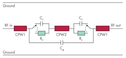
Figure 3 shows structure-based lumped-circuit models for the MEMS series switch. The contacts are modeled as resistors or capacitors, depending on the state of the switch. The lateral contact structure has two contact areasbetween the input and output ports. The coupling capacitance contains two series of capacitance Cc in parallel with capacitance Cg. Capacitance Cc is the “off”-state capacitance due to the distance between the overlapping part between the switch’s contact plate and each broken signal line.
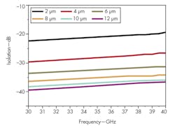
Capacitance Cg refers to the signal-line coupling capacitance due to the gap between each broken signal line. Resistance Rc is one-half of the contact resistance when the switch is in its “on” state. The switch’s “on” and “off” states are equivalent to switching between Rc and Cc. The isolation of the switch’s “off” state increased with an increase in the contact gap between the switch’s RF contact plate and the signal line, as shown in Fig. 4.
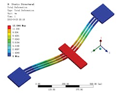
Switching between the two states is done by means of a cascaded electrothermal buckle-beam actuator. Figure 5 shows the actuator design, where three V-shaped actuator beams of the same dimension are cascaded. The width of the contact beam (W1) is 60 μm. Eachsingle bent beam has a length Lt of 400 μm, a width W2 of 10 μm, and beam angles α equal to 7deg.These parameters were chosen based on optimization of a mathematical model.
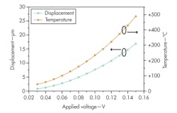
The finite-element method (FEM) method with HFSS software was used to analyze the thermal actuator. The effects of temperature-dependent material properties and thermal radiation were ignored. Figure 6 shows the simulation results of displacement and temperature versus driven voltage for the thermal actuator. Figure 7 shows that the contact point can achieve a displacement of more than 12 μm by means of a voltage of 0.12 V.
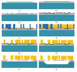
The simulated MEMS switch was manufactured using MetalMumps technology.4 The switch was fabricated on a high-resistivity silicon substrate (with resistivity of greater than 4000 Ω-cm). Figure 8 shows the process flow for the fabricated switch. In this flow, 2-μm-thick oxide was grown on the surface of the starting n-type (100) silicon wafer (a). This is followed by deposition of a 0.5-μm-thick sacrificial phosphosilicate glass (PSG) layer (Oxide 1). Wet chemical etching was used to remove the unwanted sacrificial PSG. Oxide 1 also defines the regions in which the silicon trench will be formed.
In this process flow, two 0.35-μm-thick layers of silicon nitride were deposited as mechanical support to link the actuator and the contact plate (b). Then, RIE etching was performed to remove nitride from the patterned areas where not needed (c). Following this, a second sacrificial layer (Oxide 2), 1.1-μm-thick PSG, was deposited and wet etched and a thin metal layer was deposited (d). In the next step (e), the plating base layer, consisting of 500-nm Cu + 50-nm Ti, was deposited (not shown in Fig. 8).
The wafers were coated with a thick layer of photoresist and patterned to form a stencil for the electroplated metal layer. Nickel was then electroplated to a nominal thickness of 20 μm into the patterned resist stencil (f). The photoresist stencil was then chemically removed (g). A 1 to 3 μm gold layer (sidewall metal) was electroplated to provide a low resistance contact (h). Then, a 49% HF solution was used to remove the PSG sacrificial layers (Oxides 1 and 2) and the oxide layer over the trench areas (i).
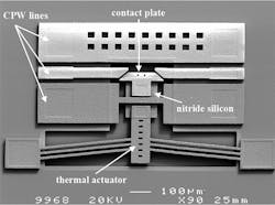
Finally, a KOH silicon etch was used to form a 25-μm-deep trench in the silicon substrate in the areas defined by the Oxide 1 (j). The SEM image for the fabricated switch is shown in Fig. 9, with a gap between the signal lines of 100 μm. The entire switch measures about 0.7 x 0.8 mm2.
Gold (Au) was chosen in this process as the contact metal because of its low resistivity, good stability, and high efficiency for RF signal propagation. The main problem with Au is its propensity toward high adhesion, which may lead to failure if restoring forces are not large enough to break a contact.5 Due to the large restoring force of the MEMS switch, no adhesion-related problems should be experienced.
This file type includes high resolution graphics and schematics when applicable.
Final Assessments
This file type includes high resolution graphics and schematics when applicable.
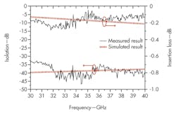
The electrical performance of the fabricated switch was evaluated under atmospheric conditions using a model N5244A PNA-X vector network analyzer (VNA) from Agilent Technologies, and 150-μm-pitch ground-signal-ground (GSG) coplanar probes from Cascade Microtech. A short-open-load-through (SOLT) standard on-wafer calibration technique was employed to set up the test system. Figure 10 shows simulated and measured S-parameters. The simulated insertion loss was less than 0.2 dB over all bandwidths from 30 to 40 GHz, with simulated isolation of better than 37.5 dB. The measured insertion loss was less than 0.3 dB, with measured isolation of better than 33 dB.
As Fig. 10 shows, the measured insertion loss and isolation show only small deviations across frequency. The discontinuity induced by the cascaded CPW lines, which have different dimensions at input and output ports, may result in the deviations. Overall, the measured S-parameters agree well with the simulated S-parameters.
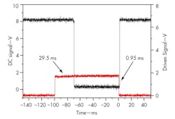
The DC characteristics were tested as follows. The 10-Hz, 1.8-V sawtooth waves for the actuation voltage test and the 1-Hz, 8-V square waves for the switching time test were supplied by a model 33220A function/arbitrary waveform generator from Agilent Technologies and a model BA4825 high-speed bipolar power amplifier from NF Corp. Both the drive signal and test signal were observed and compared by the UNI-T UTD2052CEL digital storage oscilloscope from Morton Controls. Figure 11 shows the measurement results of the switching time testing. The actuation time was 29.5 ms for the transition from the “off” to the “on” state, and the releasing time was 0.95 ms for the transition from the “on” to the “off” state.
The speed of operation of the electrothermally actuated switch was slower than switches actuated by electrostatic force. The use of electrothermal actuation is expected to provide a high-force contact, which is important for reducing the contact resistance of the MEMS switches with high restoring force. The actuation time is longer than the release time, since the electrothermal actuator generates movement through an expansion of materials caused by the Joule effect, which has a long actuation time.However, once the voltage was removed, the actuator begun to cool down, and the switch makes the transition from “on” state to “off” state fairly quickly.
The high spring constant of the nickel beams is another important factor that helps the switch reach the “off” state quickly. Although the switching time of the proposed switch is longer than its electrostatic counterparts, it could find several applications where the switching time requirement is less stringent. Examples include redundancy networks, multiband receiver band selection networks, and automated test equipment.
The objective of this research was to design a high-performance MEMS switch for millimeter-wave communication applications. The result of the work is a switch actuated byan electrothermal actuator with better than 0.2-dB insertion loss from 30 to 40 GHz and more than 33-dB isolation at frequencies below 40 GHz. The switch is suitable for use with many microwave components and systems, such as power source and phase shifters.
Yan-Qing Zhu, Engineer
Lei Han, Associate Professor
Jie-Ying Tang, Professor Key Laboraty of MEMS of Ministry of Education, Southeast University, Nanjing 210096, People’s Republic of China, +0086-25-83794642-8823, FAX: +0086-25-83792939.
Acknowledgment
This work is supported by the National Natural Science Foundation of China (grant No. 61106114).
References
1. Gabriel M. Rebeiz and Jeremy B. Muldavin, “RF MEMS switches and switch circuits,” IEEE Microwave Magazine, Vol. 2, No. 4, 2001, pp. 59-71.
2. Jad Rizk, Tan Guan-Leng, Jeremy B. Muldavin, and Gabriel M. Rebeiz, “High-isolation W-band MEMS switches,” IEEE Microwave and Wireless Components Letters, Vol. 11, No. 1, 2001, pp. 10-12.
3. Y-H. Jang, Y-S. Lee, Y-K. Kim, and J-M. Kim, “High isolation RF MEMS contact switch in V-and W-bands using two directional motions,” Electronics Letters, Vol. 46, No. 2, 2010, pp. 153-155.
4. A. Cowen, B. Dudley, and E. Hill, “MetalMUMPs Design Handbook, Revision 4.0,” www.memscap.com, accessed 2nd April2013.
5. I. Schiele, J. Huber, B. Hillerich, and F. Kozlowski, “Surface-micromachined electrostatic microrelay,” Sensors and Actuators A: Physical, Vol. 66, No. 1, 1998, pp. 345-354.
This file type includes high resolution graphics and schematics when applicable.
