Turn Down the Noise with LNAs
This file type includes high resolution graphics and schematics when applicable.
The urban world is full of noise-generating electronics ranging from cell phones to WiFi routers. This fact is especially troubling for the telecommunications industry, which needs its own noisy devices to be heard amongst the crowd. To fight the ever-increasing noise floor, noise-mitigation devices like low-noise amplifiers (LNAs) are used to increase the signal-to-noise ratio (SNR) to levels that can be accepted by downstream receiver circuitry. Because every component within an electronic circuit produces noise, however, the design of LNAs requires critical analysis of each component in the LNA and receiver system. The parameters that are most useful to an LNA designer are power consumption, linearity, gain, noise figure (NF), stability, and transistor technology.
To maintain the greatest power efficiency for portable-radio designs, LNAs have to balance their gain, linearity, and NF performance with minimal power. For example, devices that have control inputs for the bias and supply inputs can control the quiescent current independently of the supply voltage. With such controls in hand, a designer is able to set the lowest voltage point for the bias and supply to achieve the necessary gain, linearity, and NF. Using a lower supply voltage also could increase the LNA’s resilience when faced with high power surges.
Instead of increasing transistor size to make an LNA circuit more robust, a designer could choose a transistor technology with a higher breakdown voltage. In this case, the typical device technologies used include silicon-germanium (SiGe) heterogeneous bipolar junction (HBT) and gallium-arsenide (GaAs) pseudomorphic high-electron-mobility transistor (pHEMT). GaAs pHEMTS tend to perform better than SiGe HBTs for survivable power metrics. However, LNA durability can be increased, thanks to the bias circuitry adjustments that tweak the internal bias under high RF-input-power conditions. Increasing resistance at either the source of a pHEMT device or the emitter of an HBT could improve power handling by dissipating power to the device.
Under wide ranges of input power, limiting distortions to the signals, or linearity, also is impacted by transistor size and technology. For low-cost and high-volume applications, like wireless local-area networks (WLANs) and Global Positioning Systems (GPSs), SiGe HBTs are often preferred. When it comes to higher-linearity demands, however, GaAs pHEMTs typically outperform SiGe devices. Linearity performance can generally be extended by scaling the transistor size and increasing the bias current, but at the cost of power efficiency. Other factors, such as device packaging, can introduce nonlinearities unless specific fabrication steps are taken. In addition, keeping the LNA gain at a low level could raise the input-referenced linearity of the circuit as a whole.
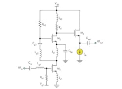
Because the gain level needs to be balanced to maintain an adequate NF, these are often competing design parameters. To optimize the NF of an LNA design, the transistor technology is again a critical choice. E-mode GaAs pHEMTs are among the highest performing in terms of NF, with SiGe HBT devices serving as the economy choice. Transistors with minimal gate or base resistance usually produce a lower NF in the final design. The footprint of the overall LNA also can influence the NF. For example, using external matching components with higher Q values generally leads to a lower NF. On-chip inductors and capacitors could provide less parasitics. For designs that are optimizing the NF, however, the significant difference in internal and external Qs makes external passives more viable (Fig. 1).
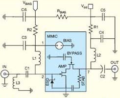
“The designer needs to know the cascaded NF of the receiver to which the LNA will be added. And the designer needs to have a clear understanding of the cascaded NF that will be required once the LNA is added,” states Alan Ake, Vice President of Applications and Technical Marketing for Guerilla RF. “This is important because it determines both the maximum allowable NF of the LNA and the minimum allowable LNA gain. In general, it is wise to keep LNA gain to a minimum, as this gain directly degrades the input-referenced linearity of the receiver as a whole.” Also among the design considerations affecting NF is the electrostatic-discharge (ESD) protection circuitry performance on the external pins of the LNA. The ESD circuitry introduces parasitic load on all of the ports. As a result, it naturally degrades the NF response at the input. The input of the LNA from the signal source also is sensitive to matching impedance, which can have an impact on the system NF (Fig. 2).
Noise matching—or matching the impedance of the LNA’s input with the signal source to reduce the NF—is a complex step in LNA design. Achieving a low level of input return loss (-10 dB, -15 dB, or better) could prevent the NF from exceeding input requirements. Resistive elements are the main contributors of noise within a circuit. As a result, only reactive elements can be used to effectively match the signal source and LNA. The best noise matching is achieved when the LNA input is the conjugate of the reflection coefficient of the transistor at the input. Often, this is different than the conjugate of S11, which is used for minimizing the input-return loss.
An inductor feedback at the source of the input transistor is frequently used to rotate the impedance closer to the reflection coefficient. This task is performed at the lowest NF possible while still offering adequate input-return loss. Ake comments, “It is very complicated, but it basically boils down to playing with the source inductance. It can be done on die, but also is done in the package with bond wires that are grounded.” In an amplifier, adding reactance at the transistor terminals also can affect the stability of the circuit. More detailed design criteria must therefore be met.
This file type includes high resolution graphics and schematics when applicable.
Stability Concerns
This file type includes high resolution graphics and schematics when applicable.
The stability requirements for LNAs dictate unconditional stability throughout the frequency range in which the amplifier has significant gain—regardless of loading conditions and temperature. This common solution reduces the gain and 1-dB compression point (P1dB) of the amplifier. Meanwhile, resistive loading at the output helps to ensure circuit stability across all frequencies. Because the resistive load is located at the LNA’s output, the effects on NF are minimal. To ensure temperature stability, the LNA circuit can be designed for stability at -40°C, as the lower temperature is often the worst case for temperature stability.
Because gain, linearity, NF, stability, and noise matching are often competing parameters, iterative design of the LNA components is critical. Modern software tools, such as Agilent’s ADS and National Instruments’ Microwave office, are used to simulate down to the transistor level. Foundries provide transistor models with noise parameters for a given technology, and these models are incorporated into the simulations. “When we simulate the noise figure of devices, it tends to be close to what we get when we implement and package them,” says Ake. “We generally have more problems with linearity simulations with what we typically build. But noise figure is often predictable.”
As integration trends continue and more advanced components can be developed on chip, monolithic-microwave integrated circuits (MMICs) are integrating more LNA circuit components. This approach is benefiting system designers, as it reduces the footprint and design complexity by removing compensation and matching components from outside the LNA chip. Advances in transistor technology also will enable lower-noise LNA technologies while pushing the boundaries of sensitivity in telecommunications receivers.
This file type includes high resolution graphics and schematics when applicable.
About the Author
Jean-Jacques DeLisle
Jean-Jacques graduated from the Rochester Institute of Technology, where he completed his Master of Science in Electrical Engineering. In his studies, Jean-Jacques focused on Control Systems Design, Mixed-Signal IC Design, and RF Design. His research focus was in smart-sensor platform design for RF connector applications for the telecommunications industry. During his research, Jean-Jacques developed a passion for the field of RF/microwaves and expanded his knowledge by doing R&D for the telecommunications industry.
