Design An ETSI E-Band Circuit
With the growing demand to wirelessly communicate voice, video, and data from point to point, effective use of European Telecommunications Standards Institute (ETSI) E-band frequencies from 71 to 76 GHz and 81 to 86 GHz has become imperative. A number of different high-frequency components are vital for building E-band communications systems, including gallium-arsenide (GaAs) pseudomorphic high-electron-mobility-transistor (pHEMT) frequency doublers, quadruplers, and power amplifiers (PAs).
Related Articles
• Antennas Reach For More Bands
• Radar Continues Scanning Outward
• Strategies for Scaling Capacity In Microwave Networks
Suitable output-power levels and power-added efficiency (PAE) are concerns for the E-band amplifiers, while power levels of +15 dBm or higher have been shown to be helpful for the local oscillators (LOs) that feed linear frequency downconverter and upconverter mixers for high quadrature-amplitude-modulation (QAM) radio systems and direct transmission for low QAM systems. Higher output power [more than +20 dBm (100 mW)] is desirable from linear E-band system PAs, with research and design communities both working toward achieving an ultimate goal of 1 W (+30 dBm) power at E-band system antennas.
In quest of circuitry for E-band systems, a grant from the Australian government brought together Australia’s Macquarie University, MACOM Technology Solutions, and WIN Semiconductors Corp. to partner on the development of a high-performance integrated-circuit (IC) process suitable for E-band use. To demonstrate its capabilities, the process was applied to the design of a Q-band-to-E-band frequency doubler and K-band-to-E-band quadrupler, including an E-band PA.
The doubler provides +15 dBm output power over the full ETSI E-bands. The quadrupler offers more power over a narrower bandwidth, as might be used for a radio system with an LO between the two E-band channels. The quadrupler delivers a maximum output level of +19.2 dBm. The PA generates more than +23 dBm (200 mW) output power over the two ETSI E-band frequency ranges, with maximum power of +24.2 dBm (265 mW).
WIN Semiconductor’s PP10 WIN process was chosen to fabricate these ICs, due to its high transition frequency, fT and high power capabilities. Unfortunately, the team had no previous experience correlating preproduction measurements of individual field-effect transistors (FETs) to production FETs, let alone to overall circuit performance, so the design and fabrication efforts would also be educational experiences.
Performance levels for the circuit designs for the doubler, quadrupler, and PA were simulated with Microwave Office® high-frequency design software from AWR Corp., using models extracted from multiple-bias S-parameter measurements on a small test transistor. The circuits were fabricated using the PP10 0.10-μm GaAs pHEMT process, with an fT of 135 GHz, transconductance of 725 mS/mm, and breakdown voltage of +9 VDC.
The doubler was a two-stage, Q-band amplifier that drove a single-ended doubling element consisting of a FET biased close to pinchoff, which in turn drove a four-stage, E-band PA. The quadrupler contained an additional K-band pre-amplifier and a K-to-Q doubling element. The output device in both circuits was a 4 x 50 μm transistor.
The power amplifier featured a four-stage, balanced topology with the final transistor in each arm being a 6 x 50 μm device customized for optimum balance among gain, channel temperature, and output power. The monolithic-microwave-integrated-circuit (MMIC) frequency doubler was 2750 x 1250 μm to fit the dicing requirements of other circuits on this wafer. The PA layout was similarly influenced by the size of adjacent circuits, and could be reduced in a production version.
A three-step process was used for the design of all circuits. In the initial step, a schematic-based circuit served as a design starting point, to provide performance levels roughly in agreement with targeted specifications. Linear design was primarily performed during this first pass, with the cursory inclusion of some nonlinear performance aspects. During the second step of the design process, individual subcircuits were laid out and the AWR EXTACT™ flow was used with the AXIEM® three-dimensional planar electromagnetic (EM) simulator from AWR to provide more accurate block-level design insights into the desired circuitry.
In the final step of the design process, critical portions of the entire chip-level metallization were run through the EXTRACT flow and compared to block-level simulations and overall target performance. Final verification of the design—including design-rule check (DRC) and layout versus schematic (LVS) operations—were performed with the AWR software before tape-out of the circuits for fabrication.
Measuring Up
For measurement purposes, a 50-GHz signal source was used to provide sufficient input power to saturate the doubler and quadrupler. Both components were both measured using wideband 50-75-GHz and 75-110-GHz power sensors. The output components included a coaxial RF probe, a waveguide transition, and a WR-10 waveguide attenuator and power sensor. The output component losses were measured using a VectorStar vector network analyzer (VNA) from Anritsu Co. with 110-GHz range.
Fundamental leakage to the power meter head was negligible, as the 75-GHz waveguide used for the attenuator and power sensor had a cutoff frequency of 60 GHz. The third- and higher-harmonic content of the doubler was believed to be negligible because of the lack of gain in the output amplifier at greater than 1.5 times the input frequency.
The doubler was used as a driver to achieve sufficient power to drive the PA into saturation. The doubler and PA were epoxied side by side on a metal block and RF/microwave connections made by means of bond wires. A three-dimensional (3D) EM simulation was used to model bond-wire losses at each measurement frequency. The specific doubler used for this test was characterized separately and the measured output power level, corrected for bond-wire loss, was used to calculate the PAE.
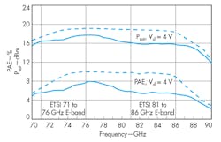
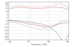
Figure 1 shows the measured and simulated results for the doubler. With a 4-V supply, the doubler provides output power above +15 dBm from 70 to 88 GHz. The PAE exceeds 4% over this same frequency band. The fundamental rejection was not measured, since the doubler’s Q-band range falls below the cutoff frequency of the waveguide used in the measurement setup.
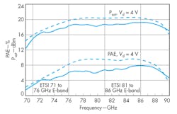
Figure 2 shows the measured output power and PAE results for the quadrupler with a +4-VDC supply, along with its simulated performance. The quadrupler offers maximum output power of +19.2 dBm at 85 GHz and delivers more than +18 dBm output power from 76 to 89 GHz. The quadrupler’s PAE exceeds 6% over this same bandwidth.
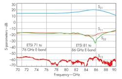
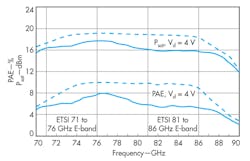
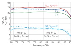
Figure 3 plots measured S-parameters for the PA, while Fig. 5 shows the PA’s measured saturated output power and PAE as functions of frequency for drain-source voltages (VDS) of +3 to +5 VDC. At the higher drain potential, the saturated output power reaches as high as +24.2 dBm (265 mW) and at least +23 dBm (0.2 W) from 71 to 86 GHz. For a +4-VDC drain potential, the PAE exceeds 8% from 71 to 86 GHz.
To accurately gauge the impact of packaging on the PA, a 3D EM simulator was used to calculate the impact of the bond wires on amplifier performance, and that simulation data was then integrated into the Microwave Office simulations. The full chip was developed as a computer model with the aid of AWR’s Analyst™ 3D EM analysis software, which uses the finite-element method (FEM) of analysis. These simulated results, shown in Fig. 4, compare favorably with measured data. Variations between the simulations and measurements can actually be traced to the semiconductor wafers themselves, which have nominal thickness of 50 μm for this process. The measured wafers were close to the edge of the process window, a major factor for the shift in performance between simulations and measurements.
Assessing The Impact
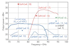
The E-band circuit’s PA power produced a peak output level of +24.2 dBm from a 600-μm periphery, corresponding to a power density of 440 mW/mm. It exceeded the 219 mW/mm power density reported for a 0.-1μm GaAs pHEMT amplifier with 640-μm output periphery and was similar in performance to the 415 mW/mm reported for a PA with smaller 100-μm output periphery. This suggested that the transistor combination used here had not resulted in significant power loss. These GaAs power densities were less than the values of 1400 to 1667 mW/mm reported for more expensive gallium-nitride-on-silicon-carbide (GaN-on-SiC) processes.
The PA was laid out with resistors in the drain bias supply lines as a conservative measure to provide additional stability margin for low-frequency operation. This reduced the drain efficiency of the PA’s last stage from an intrinsic value of approximately 35% to an extrinsic value of about 27%. The drain supply line resistors reduced the PAE by approximately two percentage points. The simulated performance for the PA was in good agreement with measured levels for both saturated output power and PAE (Fig. 5).
The simulated and measured data also agree rather well for the doubler and quadrupler circuits (Figs. 1 and 2), which is somewhat remarkable given the project team’s lack of familiarity with a new semiconductor process. Furthermore, considering that the models used for the simulation were based on a single model fit to a broad frequency range—in addition to a high dynamic range encompassing extremely linear conditions to highly nonlinear performance—the agreement in Fig. 1 is truly outstanding.
In particular, for the quadrupler this includes HEMTs operating in Class-A linear and saturated modes at K-band frequencies; a K-to-Q-band frequency-doubling HEMT device operating near pinchoff with low drain potential; HEMTs operating in Class-A linear and saturated modes at Q-band frequencies; the Q-to-E-band frequency-doubling HEMT device operating near pinchoff with low drain potential; and HEMTs operating in Class-A linear and saturated modes at E-band frequencies.
Considering the performance levels of these devices, the agreement shown in Fig. 2 is not only reasonable but also quite good in its own right. Note that a small discrepancy in the logarithmic output power simulation led to a larger discrepancy in the PAE being a linear metric. A similar instance applied to the frequency doubler in Fig. 1.
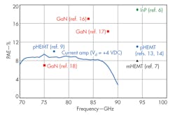
7. These curves compare the PA’s PAE (solid line) with published PAE results for the GaAs pHEMT amplifier (blue lines and circles), the black triangle is the mHEMT amplifier (black triangles), the green diamond is the InP amplifier (green diamond), and the red line and squares are the GaN amplifier (red line and squares).
Figure 6 shows the measured output power for the PA in comparison with circuits at E- and W-band frequencies, with output power of 100 mW (+20 dBm) or more. The PA has a 3-dB power bandwidth limited by the measurement setup to 18 GHz (23%) compared with 13 GHz for the GaN amplifier documented in Fig. 6. The PA’s output-power performance compares with other semiconductor approaches, as shown in Fig. 6. Finally, Fig. 7 provides an indication of the DC power required for the amplifier, in terms of its PAE, with data points reported for the comparison processes.
Related Articles
• Antennas Reach For More Bands
• Radar Continues Scanning Outward
• Strategies for Scaling Capacity In Microwave Networks
In summary, the E-band circuit combined a frequency doubler, quadrupler, and PA with good results. The doubler offers broadband output power of better than +15 dBm while the quadrupler achieves maximum measured output power of +19.2 dBm. The PA, which exceeds the +23-dBm (200-mW) specification across the entire 15-GHz ETSI E-band bandwidth, offers maximum measured output power of +24.2 dBm (265 mW).
The PA’s measured PAE is above 8% across the ETSI E-band frequencies, which is the highest saturated output power and PAE for a PA spanning the full 71-to-86-GHz range of the ETSI E-band specification for any semiconductor system. The first-pass success of this design effort represents a major step forward in the industry’s ability to deliver 1 W radiated power from a single-chip solution in an E-band system.
Dr. Michael Heimlich, Technical Marketing Consultant
AWR Corp., 1960 E. Grand Ave., Ste. 430, El Segundo, CA 90245; (310) 726-3000, FAX: (310) 726-3005.
Acknowledgements
The author would like to thank the following for their contributions to the design effort and this article: Anthony E. Parker, Department of Engineering, Macquarie University; Melissa C. Rodriguez, Jabra Tarazi, Anna Dadello, Emmanuelle R.O. Convert, MacCrae G. McCulloch, Simon J. Mahon, Steve Hwang, Rodney G. Mould, Anthony P. Fattorini, Alan C. Young, and James T. Harvey of the Sydney Design Centre; MACOM Technology Solutions, Australia; and Wen-Kai Wang of WIN Semiconductor, Taiwan.
