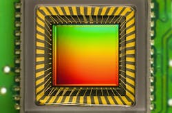
Probing Those Tiny Millimeter-Wave ICs
Semiconductors, notably integrated circuits (ICs), are helping electronic design engineers in general to achieve unprecedented levels of miniaturization with multiple-function circuits, be they combinations of components or complete receiver/transmitter front ends. Of course, such miniaturization also carries the challenge of testing these circuits, and the first look at a measurement for one of these ICs may be on a wafer or in die form.
Testing is no longer the simple practice of running a test cable between a coaxial component and the test port of a vector network analyzer (VNA). When it comes to testing at the chip level, it is time to get to know more about on-wafer probes.
Wafer probes make it possible to know the performance of an IC without its package. An effective wafer probe can measure the electrical performance of an IC without inflicting physical damage on the IC. But selecting a wafer probe is no simple matter, since each probe has a set of both electrical and mechanical characteristics that need to be matched to a particular circuit or device to be tested.
And with the growing need for testing electronic circuits for millimeter-wave circuits in Fifth-Generation (5G) wireless network equipment and automotive radar systems, the right wafer probe must do more than deliver outstanding electrical performance that doesn’t stand in the way of its companion VNA. It also must hold up over time and with the many thousands of placements required to test extremely fine-dimensioned circuits, both in the lab and on production lines.
The probe tips of high-frequency wafer probes are fabricated with the same precision as they semiconductor devices they test. Ideally, they can make contact with a conductor or active area of a semiconductor at a single point, without need for ground. More typically, probe tips are designed with multiple contact points to accommodate signal, test, and power contacts. Probe layouts are in different configurations, such as ground-signal-ground (GSG), ground-signal (GS), and signal-ground (SG) layouts, depending upon the circuit to be tested.
A key to achieving good probe performance is the electrical transition from the probe tip to the other side of the probe, which connects to the test equipment. The transition may be in the form of a particular transmission-line configuration, such as coplanar waveguide (CPW), which can transfer signals from the probe tip to the interconnection for the VNA or other test equipment, whether it is a coaxial or waveguide connector (depending upon frequency).
Wafer probes are characterized by a unique set of parameters. The contact area provides an idea about the smallest circuit dimensions that can be probed. The contact resistance describes the electrical effects of the probe’s contact point on the signal path between the circuit under test and the VNA’s input ports. The means by which a probe tip makes contact with a circuit’s conductor surface, such as a spring-loaded mechanism, can determine the effectiveness of a probe in making contact with nonplanar circuit surfaces. In addition to a probe’s frequency range, other important parameters include its insertion and return losses, type of input connectors (such as coaxial connectors or waveguide), and repeatability over long operating lifetimes, such as a million or more contact cycles.
Some details which are not always obvious on a wafer probe data sheet—e.g., whether a probe’s probe tips are clearly visible during testing for ease and accuracy of manual placement on a circuit—can be just as important when choosing a wafer probe, especially for the small dimensions of millimeter-wave circuits.
Fortunately, a number of companies, such as Cascade Microtech and GGB Industries have been in the business of designing and manufacturing high-frequency test probes for some time. Both firms offer coaxial wafer probes to 110 GHz, and Cascade features waveguide wafer probes for measurements well into the upper millimeter-wave frequency range. With increasing activity at millimeter-wave frequencies, and the inevitable growth of electronic devices and circuits at those frequencies, wafer probes are about to become standard equipment for many test stations.
About the Author
Jack Browne Blog
Jack Browne, Technical Contributor, has worked in technical publishing for over 30 years. He managed the content and production of three technical journals while at the American Institute of Physics, including Medical Physics and the Journal of Vacuum Science & Technology. He has been a Publisher and Editor for Penton Media, started the firm’s Wireless Symposium & Exhibition trade show in 1993, and currently serves as Technical Contributor for that company's Microwaves & RF magazine. Browne, who holds a BS in Mathematics from City College of New York and BA degrees in English and Philosophy from Fordham University, is a member of the IEEE.


