This file type includes high resolution graphics and schematics when applicable.
Direct-digital-synthesizer (DDS) frequency sources continue to gain in speed. This progression is epitomized by the new model AD9914 DDS from Analog Devices (www.analog.com), capable of operating at clock frequencies to 3.5 GHz. The DDS integrates a 12-b digital-to-analog converter (DAC). The AD9914 can deliver clean analog output waveforms to about 1.4 GHz, with outstanding spurious-free dynamic range (SFDR) and excellent phase-noise performance. With its unique 32-pin parallel port, which supports parallel or serial programming of the AD9914, the DDS provides a user with complete control of amplitude, phase, and frequency in order to generate advanced modulation formats with precision and speed.
1. The AD9914 is a high-speed direct-digital synthesizer (DDS) capable of operating at clock frequencies to 3.5 GHz.
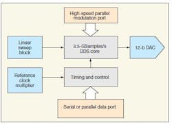
The AD9914 is a “building-block” source, housed in a compact 88-lead LFCSP package (Fig. 1) that is powered by +1.8- and +3.3-VDC supplies and ready to be programmed for the many capabilities of a DDS. It can perform any number of linear and nonlinear sweep (in frequency, phase, and/or amplitude) functions, making it a powerful source engine for test equipment, commercial and military communications systems, and radar systems. With its integrated 12-b DAC (Fig. 2), it is capable of frequency tuning resolution of 190 pHz and better. The DAC provides analog outputs from DC to 1750 MHz as balanced signals with two outputs.
2. This simplified block diagram shows the main function blocks of the AD9914 DDS.
The AD9914 features a digital ramp generator (DRG) that allows linear modulation of frequency, phase, or amplitude. The core of the DRG is a 32-b accumulator clocked by a programmable timer. The time base for the timer is the DDS clock, operating at 1/24 times the system clock. The timer establishes the interval between successive updates of the accumulator.
The AD9914 can also be used in programmable modulus mode, providing a significant increase in frequency resolution and allowing for output frequencies that are an exact, arbitrary integer submultiples of the sampling frequency (1/10, for example). Conventional DDS architectures provide power-of-2 integer submultiples of the sampling clock frequency.
The hallmark feature of the AD9914 is its 32-pin parallel port, which allows for serial or parallel programming of the device’s control registers or for providing direct access to the three DDS control parameters: frequency, phase, and amplitude. The latter provides for unprecedented speed and flexibility in terms of modulating the DDS’ output waveforms.
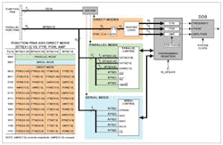
Figure 3 shows a block diagram of the parallel-port architecture. The 32-pin parallel port works in conjunction with an independent set of four function pins, controlling how the pins of the parallel port are used. The relationship between the function pins, F[3:0], and the parallel-port pins, BITS[31:0], appear in the table within Fig. 3.
3. A special feature of the AD9914 is its 32-pin parallel port, which allows for serial or parallel programming of the device’s control registers or for providing direct access to DDS frequency, phase, and amplitude.
When the logic levels applied to the function pins are such that F[3:0] = 0000, the 32-pin parallel port functions as a parallel interface to all of the device programming registers via the “Parallel Mode” block in Fig. 3. When the logic levels applied to the function pins are such that F[3:0] = 0001, the 32-b parallel port becomes a serial interface to all of the device programming registers via the “Serial Mode” block in Fig. 3. In this case, only the five lowest-order pins of the 32 are functional. When the logic levels applied to the function pins are any other combination (except 1110 and 1111, which are not used), the 32-pin parallel port has direct access to the DDS core via the “Direct Modes” block in Fig. 3.
Using the Direct Modes functionality gives the parallel port direct access to the 32-b frequency, 16-b phase, and 12-b amplitude parameters of the DDS core. The table within Fig. 3 details how the 32 pins of the parallel port map to the frequency (FTW), phase (POW), and/or amplitude (AMP) parameters of the DDS. The Direct Modes functionality gives the AD9914 unprecedented modulation capability because it gives the user direct access to the DDS core for high-speed control of frequency, phase, amplitude, or various combinations thereof. This is because the parallel port operates at a sample rate equal to 1/24 of the system sample clock, so frequency, phase, and/or amplitude changes to the DDS output signal can occur at rates to 145 MSamples/s (assuming a 3.5-GHz system clock). As such, the AD9914 can accommodate virtually any application requiring wideband modulation of frequency, phase, and/or amplitude.
For flexibility, the AD9914 incorporates a reference clock multiplier that allows lower-frequency clock sources to be used. The clock multiplier provides multiplication factors from 8x to 255x with an internal phase-lock-loop (PLL) multiplier.
In Direct Modes operation, frequency, phase, and amplitude data travel to the DDS core over different paths with different propagation times (latency). Modulating more than one DDS parameter necessitates setting the DDS’ matched latency bit, which equalizes the latency of each DDS parameter as it propagates from the parallel port to the DDS core. High-speed modulation will require a DAC reconstruction filter with sufficient bandwidth to accommodate the instantaneous time-domain transitions.
With 32-b frequency control, 16-b phase tuning, and 12-b amplitude scaling, the DDS provides almost complete control of an output waveform, enabling frequency-agile programming, amplitude shift modulation, and virtually any form of frequency- or phase-based modulation, such as frequency-shift-keying (FSK) or phase-shift-keying (PSK) modulation. For simplified output shift keying (OSK) functionality, the AD9914 has a separate OSK block that affects only the amplitude parameter of the DDS. The OSK function has priority over the other data sources that can drive the DDS amplitude parameter. As such, no other data source can drive the DDS amplitude when the OSK function is enabled.
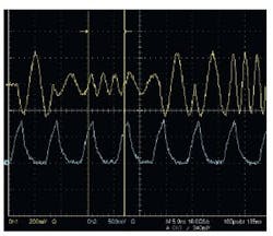
4. This oscilloscope screen displays the high-speed modulation capability of the AD9914, with the bottom trace the SYNC_CLK output of the AD9914 at a 145-MSamples/s input sampling clock rate, and the top trace the raw output of the AD9914 without a DAC reconstruction filter.
In terms of output waveform performance, the AD9914 features better than -50 dBc wideband SFDR, with typical phase noise of -128 dBc/Hz offset 1 kHz from a 1.396-GHz carrier. Figure 4 illustrates the high-speed modulation capability of the DDS. The synthesizer is operating at a sampling clock rate of 3.5 GHz and data update rate of 145 MSamples/s (a period of 6.9 ns, as indicated by the oscilloscope’s vertical markers). The bottom trace shows the SYNC_CLK output of the AD9914, showing the 145-MSamples/s input sampling clock rate. The top trace shows the raw DAC output of the AD9914, without a DAC reconstruction filter. At the start of each cycle of SYNC_CLK, the F[3:0] and BITS[31:0] pins are driven externally to select the desired DDS parameter (frequency, phase, or amplitude). Table 1 provides details on the parameters used to generate the modulation states.
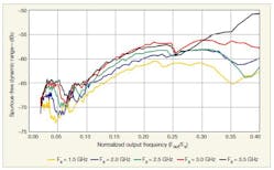
Frequency-domain performance was evaluated at several different clock frequencies (Fig. 5). Each trace shows the SFDR performance for the AD9914 at system clock rates from 1.5 to 3.5 GHz. The traces are shown as normalized output frequencies—that is, as a fraction of the system clock frequency since each trace represents a different system clock frequency. As these plots show, for system clock frequencies from 1.5 to 3.5 GHz, the AD9914 delivers typical SFDR performance of -65 dBc for output frequencies to 10% of the system clock (e.g., as high as 350 MHz at a clock rate of 3.5 GHz). Even for output frequencies as high as 1 GHz (or approximately 30% of a 3.5-GHz system clock frequency), the SFDR is typically better than -56 dBc.
5. This is the typical spurious-free-dynamic-range (SFDR) performance possible with the AD9914.
The AD9914’s frequency-domain performance can also be evaluated in terms of additive phase noise, which is critical to the performance of many modern communications systems—especially those using digital modulation schemes. The typical phase-noise performance of the AD9914 DDS is reported in the table for carrier frequencies from 171 to 1396 MHz and at offsets from 10 Hz to 10 MHz, using a sampling clock frequency of 3.5 GHz. Close-in phase noise, offset just 10 Hz from the carrier, is quite good for a digital synthesizer, at -125 dBc/Hz for a 171-MHz carrier and still only -109 dBc/Hz for a 1.396-GHz carrier. Closer to the noise floor, the phase noise is -158 dBc/Hz offset 10 MHz from a 171-MHz carrier and a quite-respectable -145 dBc/Hz offset 10 MHz from a 1.396-GHz carrier. Table 2 shows typical phase-noise values at these and other carriers for offset frequencies from 10 Hz to 10 MHz.
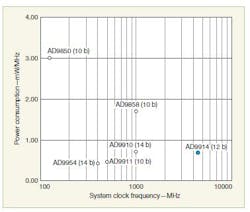
Given the amount of functionality designed into the AD9914, along with its maximum system clock rate of 3.5 GHz, one would expect the device to be power hungry. Figure 6 indicates otherwise, as it plots power consumption per maximum system clock frequency (mW/MHz) for several different DDS devices in ADI’s DDS portfolio, showing the AD9914 is on par with the other DDS products in the AD99xx series. The AD9914 typically consumes 2.4 W when operating at a 3.5-GHz clock rate. Note the chart also indicates the DAC resolution for each DDS device.
6. Power consumption for the AD9914 DDS is plotted as a function of system clock frequency.
The AD9914 can save power by using a programmable power-down mode, without necessarily losing a great deal of functionality because of its switching speed: The AD9914 requires only 45 ns to enter power-down mode, and only 250 ns to leave power-down mode. The DDS is designed to handle operating temperatures from -40 to +85°C operating temperature range, and offers the programmability and performance to meet the needs of applications that might have formerly relied on analog signal sources. P&A: $159.50 each (100 qty.); 10 to 14 wks.
Analog Devices, Inc., One Technology Way, P.O. Box 9106, Norwood, MA 02062-9106; (781) 329-4700, (800) 262-5643, e-mail: [email protected], www.analog.com.
This file type includes high resolution graphics and schematics when applicable.
