This file type includes high resolution graphics and schematics when applicable.
Firas Mohammed Ali
Al-Raie
Department Head
The Polytechnic Higher Institute of Yefren, Libya,
Department of Electronic Engineering,
e-mail: [email protected]
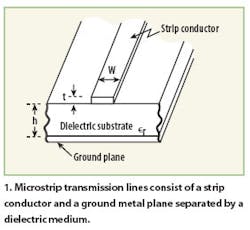
Microstrip lines are commonly used in microwave circuits, although their performance is subject to the type of substrate material selected for a printed-circuit board (PCB). One of the more important material parameters for the substrate is the relative dielectric constant, which should be known before designing a high-frequency, microstrip-based circuit. What follows is a simple and practical method for estimating the relative dielectric constant of a microstrip substrate based on well-known microstrip line empirical equations.
where:
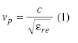
c = the speed of light and ere = the effective dielectric constant of the microstrip line.
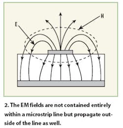
The value of ere is significantly lower than that of er when the fields external to the substrate are taken into account. The guide wavelength, λg is related to the free-space wavelength, λ, as shown by Eq. 2:
Available numerical methods for the characterization of microstrip lines involve extensive computations. Closed-form expressions are necessary for the computer-aided design (CAD) and optimization of microstrip circuits. The closed-form expressions for Zo and ere apply to the following two sets of conditions2:
For W/h ≤ 1,
where:
And for W/h ≥ 1,
where:
These expressions provide accuracy of better than 2 percent.
Strip thickness
The results discussed above assume a negligible strip thickness. In reality, the thickness of the strip has some bearing on the electrical performance, and the strip thickness, t, affects the microstrip characteristics. However, for a thickness- to-height ratio (t/h) less than or equal to 0.005, the agreement between experimental and theoretical results obtained by assuming t/h = 0 is acceptable.2
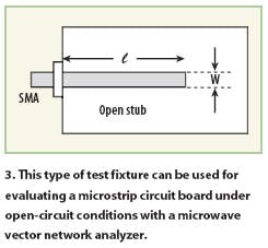
If the substrate thickness, h, of the circuit board is known, then the relative dielectric constant of the board can be determined using a simple experiment. This involves placing the test microstrip circuit board with specific length, l, and width, W (where W > h) into a test fixture and evaluating the microstrip circuit board under open-circuit conditions over a specified range of frequencies. Figure 3 offers an example of a test fixture for this purpose. The input impedance (or reactance) of the line should be recorded for each sample frequency.
It is well known that the input admittance of an open-circuited stub is given by:
The characteristic impedance of the open-circuit microstrip line is:
where Xoc is the measured input reactance of the microstrip line at the specified frequency (assuming it to be lossless).
Substituting Eq. 2 in Eq. 8 yields:
where:
λ = c/f
For a microstrip line with W/h ≥ 1, Zo is given by Eq. 5 and can be rewritten as:
and ere is given by Eq. 6 as:
where:
and
Substituting Eq. 11 into Eq. 10 and equating Eqs. 10 and 8 yields:
To find er, Eq. 14 can be solved using the Newton-Raphson iterative formula. Thus, Eq. 14 can be formulated as:
A computer program can be written to minimize f (er) according to the algorithm:
where:
and where ere is substituted from Eq. 11. An initial value of er close to the actual value is necessary for the algorithm to converge as quickly as possible.
This estimation procedure was used to determine the relative dielectric constant for two types of substrate materials: Teflon-fiber glass (PTFE) and epoxy-glass boards. The relative dielectric constant of the PTFE substrate was found to be 2.68. This value is approximately constant over a wide range of frequencies. The microstrip line for this type of substrates can be considered lossless at frequencies to several gigahertz.
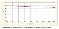
On the other hand, the relative dielectric constant of the epoxy-glass substrate was found to be dependent upon frequency. Figure 4 shows the variation of er with frequency for this type of substrate. It was also found that losses in the epoxy-glass board make it impractical for applications above 500 MHz.
As a conclusion, this simplified method can be readily used to determine the relative dielectric constant of a microstrip substrate using a variety of different substrate materials. The approach is based on measuring the input reactance of an open-circuit microstrip line with the aid of a vector network analyzer (VNA) at a specified frequency. The classic microstrip-line equations found in the literature were formulated as a root finder algorithm to search for er.
REFERENCES
1. G. Gonzalez, Microwave Transistor Amplifiers Analysis and Design, 2nd ed., Prentice-Hall, Upper Saddle River, NJ, 1997, Chapter 2.
2. I.J. Bahl and D.K. Trivedi, "A Designer's Guide to Microstrip Line" MicroWaves, May 1977, pp.174-182.
