Analog signals are often digitized as quickly as possible in modern communications systems and test equipment in order to perform signal processing in the digital domain. But designing the transformer frontend circuitry for an analog-to-digital converter (ADC) can be challenging, especially in systems with high intermediate frequencies (IFs). Fortunately, this streamlined, five-step process can help develop an optimum front end for an ADC. It can be applied easily and quickly to achieve the desired performance in almost any application.
The five-step process is based on a straightforward and logical procedure:
1. Know the system and the design requirements.
2. Determine the ADC's input impedance.
3. Determine the ADC's baseline performance.
4. Select transformer and passive components to match the load.
5. Bench test the design.
For example, the first step sounds obvious, but just knowing the requirements of a particular application can quickly cut down the number of iterations that must be done, selecting the right components from the start and quickly achieving the desired performance. Make a list of each design requirement, and set desirable boundaries to work within. This will enable selection of the ADC and transformer to go quickly.
Using an example, assume an application that requires a sampling rate of 61.44 MSamples/s to capture input signals across a 20-MHz band centered at 110 MHz (100 to 120 MHz). The required signal-to-noise ratio (SNR) of better than 72 dB implies the use of a 14-b ADC to provide the needed SNR performance. The power consumption should be less than 500 mW per channel. A quick search for an ADC that can meet these system-level performance requirements led to the 14-b, 80-MSamples/s model AD9246 ADC from Analog Devices designed to run on supplies from 1.8 to 3.3 V. The device was selected for its wide bandwidth and low power consumption (Table 1).
In this example design, the ADC will be fed with an input 110-MHz IF with 20-MHz bandwidth and 61.44MSamples/s sampling rate. Since the bandwidth is narrow (one Nyquist band), a resonant match technique is used. This type of match provides less bandwidth, but allows excellent matching over the specified frequency range. This technique usually requires the addition of an inductor or ferrite bead directly across the analog inputs to resonate the parasitic capacitance away from what is seen by the ADC's input stage. If the IF of interest is in baseband (first Nyquist), then a lowpass filter can be derived using a simple RC network.
The second step in the process involves finding the ADC's input impedance (Fig. 1). The device in question, the model AD9246, is an unbuffered or switched-capacitor-type ADC. This means that the input impedance is time varying and changes with respect to analog input frequency. To determine the input impedance for this device, the spreadsheet on the AD9246's product page can be used (which can be located at: http://www.analog.com/en/prod/0, 2877,AD9246,00.html). From that spreadsheet, it is simply a matter of finding the impedance measured at 110 MHz in the track mode. In this example, the ADC's internal input load looks like a differential 6.9-kW resistor in parallel with a 4-pF capacitor. It is best to match in the ADC's track mode, as this is when the ADC is actually taking the sample. Table 2 shows a portion of the spreadsheet from the AD9246's product page.
The third step involves determining the ADC's baseline performance in order to better understand how the ADC behaves before trying to optimize all of its design parameters. To establish this reference, use the evaluation board as configured in its default condition. This is most likely how the ADC was characterized for the specifications shown on the product datasheet.
Next, start gathering the performance specifications. This can be achieved by collecting a Fast Fourier Transform (FFT) with a 110-MHz input frequency at –1 dB full scale (dBFS), yielding an SNR of 72 dB and an spurious-free dynamic range (SFDR) of 82.7 dBc, close to the datasheet specifications. Characterization should be performed with a high-performance signal generator and filter to clean up any signal-generator harmonics and spurious content when performing the testing.
Following this, the filter is removed and the ADC's evaluation board is reconnected to the test signal generator. The output level of the generator should be readjusted and noted, in this case +14 dBm, in order to collect the input drive number. The input frequency should be swept over enough bandwidth to see how the passband flatness changes and to achieve the –3-dB points.1 In this case, the front-end default configuration has a simple RC filter which makes for a passband flatness of 1.2 dB and a bandwidth of about 100 MHz.
Now that this data has been collected, it is time to make some decisions. With a requirement of 72 dB SNR and 83 dBc SFDR, it is essential that an anti-aliasing filter (AAF) be used to improve the spurious performance and keep the signal harmonics low. This still doesn't solve the input drive and passband flatness issues, however. The AAF on the default evaluation board quickly attenuates the passband of interest. Using a simple shunt inductor can help, as it will provide less attenuation at the frequency of interest, and it rolls off more graciously outside the band. For the input drive, a 1:4 transformer will be considered to achieve the full-scale of the ADC. This will gain the signal by +6 dB, thus offsetting the input drive requirement even more. Finally, the input impedance and VSWR should be measured with a vector network analyzer (VNA). Dial-in the frequency of interest to see how well the input matches. In this case of this example, 35 ohms was measured at 110 MHz, yielding a VSWR of 1.44:1.
The fourth step involves selecting the transformer and passive components to match the impedance of the load. In the previous step, the foundation was laid by creating a baseline. Next, the transformer and component values for both R and L must be selected to match the load and create a new AAF that will achieve the desired overall performance between the ADC and secondary of the transformer (Fig. 2).
This is where experience or experimentation can come into play. Selecting the transformer can prove to be difficult, since the performance of different transformers can vary widely. The transformer for this example was chosen because it has been measured and its capabilities are understood. In general, it is important to choose a transformer with a good phase imbalance characteristic. This example application has a narrow bandwidth and requires a low input drive, so a known transformer with a 1:4 impedance ratio will be used.
Some simple guidelines on choosing a transformer for an ADC include a close look at the specifications. For example, the return loss, insertion loss, and phase and magnitude imbalance specifications should be carefully compared. If these parameters are not specified on the data sheet, ask the manufacturer for this data, or measure it using a vector network analyzer. Choosing between a standard flux-coupled transformer or balun is really a matter of meeting the bandwidth requirements. Standard transformers tend to be in the 1-GHz or under region, whereas a balun can achieve much higher bandwidth.
Note that the termination could be split between the primary and secondary, but in this case only the secondary was terminated in order to minimize the number of components required. Depending on the application, a split termination may make more sense.
Small series resistors should be used on the analog inputs, about 15 to 50 ohms. In this case, two 33-ohm resistors were used. The reason for this is to limit the amount of charge injection from the unbuffered ADC back onto the analog inputs. This also helps to define a certain amount of source resistance from the preceding stage. In 90 percent of the cases, 33 ohms can be used, but in some cases, varying this value has proven to increase the performance slightly.
Next, solve for the differential termination on the secondary of the transformer. As the calculation shows, below 251 ohms is a good starting point for the secondary differential termination. 200 ohm would be used with an ideal 1:4 impedance ratio transformer. To start the calculation, use the return loss number at the specified center frequency to calculate the actual characteristic impedance (Z0).
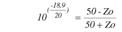
Here is an example of a calculation for the secondary termination of the transformer. The return loss is found as
Return Loss (RL) = –18.9 dB @ 110 MHz = 20log(50 – Z0/50 + Z0),
Using this value of the return loss, it is possible to solve for the characteristic impedance of the transformer's secondary by:
where:
Z0 = 39.8 ohms.
In an ideal 1:4 impedance transformer, 200 ohms on the secondary should equal 50 ohms on the primary. This is not the case in a real system, however. To determine the real impedance reflected back to the primary is, use the value of Z0 found in the previous step and follow the simple calculation below.
solving for X, X = 251 ohms
Since the transformer will have some unaccounted losses, the 251-ohm secondary termination will make up for these losses. This sets up a better termination value to start with on the secondary to reflect back the correct impedance onto the primary of the transformer. In this case, 50 ohms is stated by the design requirements.
Next, the value of the inductance, L, must be determined to resonant away the internal ADC parasitic capacitance. This can be done by setting the value of capacitance, C (4 pF), to the value of L.
As an example calculation for the inductor, L:
1/(2*pi*110M*4p) = 361.7 ohms
With these values, it is now possible to solve for L:
361.7/2*pi*110M = 523 nH
The reactance of L is set to be equal to C. In the case of this example, the 4pF capacitance turns into an inductance of 523 nH at 110 MHz. This will set a starting point for the value of L.
The final step in the search for an optimum ADC transformer match is to bench test the design with the values of resistance and inductance that have been found in the earlier steps of the procedure. It is important to go back and measure each of the performance metrics, i.e., SNR, SFDR, input drive, passband flatness, and input impedance, as was done previously in the default condition to establish the ADC's baseline performance.
It is worth noting that both calculated R and L values can differ in order to get the best performance. The value of these components may vary versus what was initially calculated depending on vendor preference and component size availability. As iterations occur, a spreadsheet helps keep track of the performance metrics as they change from iteration to iteration.
For this example, with the converter at nearly full scale, the SNR and SFDR performance levels were achieved within the goals specified (Fig. 3). At 110 MHz, the SNR is nearly 72 dB while the SFDR is 80 dBc. Figure 4 shows the final performance results measured for input drive, which was +3.1 dBm. It also shows passband flatness of less than 0.5 dB over a 50-MHz band. The –3 dB bandwidth of 150 MHz is sufficient for the requirements of the example and offers adequate spurious rejection for this design.
Figure 5 shows a combination Smith chart and VSWR plot of the input design as measured by the vector network analyzer. The input impedance is roughly 41 ohms at 110 MHz. The VSWR remains close to 1.2:1 and follows the filter characteristic appropriately.
In the end, this example shows that "matching" the input circuit or ADC analog front end improves input drive, passband flatness (in the IF passband), and reflective power to the load (VSWR), while achieving the same ADC, SNR, and SFDR performance as specified in the datasheet.
An optional sixth step in the procedure involves a comparison of calculated performance with the actual measured results. The impedance results can be calculated and compared to the measured values as a check. For an example calculation of the entire input match:
XC = 1/(2pfC) = 1/(2p 110M 4p) = –361.7 ohms, ADC imaginary impedance
6.9k || 4pF or (6.9k + j0) || (0 – j361.7) = (18.9 – j361), ADC impedance
XC = 1/(2pfL) = 1/(2p 110 M 523 n) = –361.5 ohms, L imaginary impedance
(18.9 – j361) || (0+j361.5) = (6.93k + j72.8)
(6.93k + j72.8) + (66 + j0) = (6.97k + j72.8) (add two 33-ohm resistors).
The termination seen at the secondary of the transformer is:
(6.93k + j72.8) || (242 + j0) = (234 + j82.1m)
The magnitude can be found from:
(Re2 + jX2)1/2 = 234 ohms
By taking the ratio again, as in the fourth step of the procedure, 234/200 = 50/X, and solving for X, yields X = 42.7 ohm! In this case, the measured and calculated impedances were very close.
Important points to remember when handling a new design are to rank the important parameters in the design and take the time to establish good system and design requirements.
When choosing a transformer, it is important to remember that transformers have their differences and the best way to compare different components is by fully understanding the transformer specifications. If specifications are not available, ask the manufacture for parameters that are not given. Remember, high IF designs can be sensitive to transformer phase imbalance. Two transformers or baluns may be needed for very high IF designs to suppress the even order distortions.
When choosing an ADC, establish whether a buffered or unbuffered ADC will be used. Unbuffered or switched-capacitor ADCs have a time-varying input impedance and are more difficult to design with at high IFs. If using an unbuffered ADC, always input match in the track mode and use the input impedance spreadsheets available on the manufacturer's website. Buffered ADCs tend to be easier to design with, even at high IFs, although they also consume more power than unbuffered ADCs. When calculating the R and L values, remember that this proves to be a good starting point. Not all layouts and parasitics are equal on each application, so take note that some iteration may be required to finalize on the performance needed for the particular application.
REFERENCES
1. For more information on testing ADCs, please refer to AN-835.
FOR FURTHER READING
AN-742, Frequency-Domain Response of Switched-Capacitor ADCs.
AN-827, A Resonant Approach to Interfacing Amplifiers to Switched-Capacitor ADCs.
ADC Switched-Capacitor Input Impedance Data (Sparameters) data for AD9215, AD9226, AD9235, AD9236, AD9237, AD9244, AD9245. Go to their web pages, click on Evaluation Boards, upload Microsoft Excel spreadsheet.
Rob Reeder, "Transformer-Coupled Front-End for Wideband A/D Converters," Analog Dialogue 39-2, 2005, pp. 3-6.
Rob Reeder, Mark Looney, and Jim Hand, "Pushing the State of the Art with Multichannel A/D Converters," Analog Dialogue 39-2, 2005, pp. 7-10.
Walt Kester, "Which ADC Architecture is Right for Your Application?" Analog Dialogue 39-2, 2005, pp. 11-18. Rob Reeder and Ramya Ramachandran, "Wideband A/D Converter Front-End Design Considerations—When to Use a Double Transformer Configuration," Analog Dialogue 40-3, 2006, pp. 19-22.
Rob Reeder and Jim Caserta, "Wideband A/D Converter Front-End Design Considerations—Amplifier- or Transformer Drive for the ADC," Analog Dialogue 41-2, 2007. Analog Devices (www.analog.com), model AD9246, 80/105-/125-Msps 14-bit, 1.8-V, switched-capacitor ADC data sheets.
Mini-Circuits (www.minicircuits.com), model ADT1-1WT datasheets.
M/A-COM (www.macom.com), models ETC4-1T-7 and ETC1-1-13 datasheets.
About the Author

Rob Reeder
Application Engineer, High-Speed Converters, Texas Instruments
Rob Reeder is currently the application engineer for high-speed converters at Texas Instruments (TI) in Dallas. Rob’s earlier experience includes RF design at Raytheon Missile Systems in Tucson, Ariz., including analog receivers and signal processing applications. He was also a system application engineer with Analog Devices in the High-Speed Converter and RF Applications Group in Greensboro, N.C., for over 20 years.
Rob has published over 130 articles and papers on converter interfaces, converter testing, and analog signal-chain design for a variety of applications. He received his MSEE and BSEE from Northern Illinois University in DeKalb, IL, in 1998 and 1996, respectively. When Rob isn’t writing papers late at night or in the lab hacking up circuits in the lab, he enjoys hanging around at the gym, listening to EDM, building rustic furniture out of old pallets, and, most importantly, chilling out with his family.
