This file type includes high resolution graphics and schematics when applicable.
Data converters provide a transition between the analog and digital signal realms. The two basic converter types, analog-to-digital converters (ADCs) and digital-to-analog converters (DACs), share many common circuit elements and even come in similar multi-pin packages. Key performance parameters are identical between the two, including clock speed, sampling rates, and bandwidth, but they differ in many other ways. Ultimately, understanding how the different characteristics can be used to describe an ADC or a DAC will help speed the task of finding an optimum data converter for a particular application.
ADCs sample continuous analog signals over an input voltage range and convert them into digital representations (words) with resolution equal to the ADC’s number of bits. Sampling occurs at the ADC’s clock frequency. DACs convert digital input code into analog output signals, essentially providing the opposite function of an ADC. Both types rely heavily on the performance of a clock oscillator (or oscillators) to achieve the most precise and repeatable sampling process.
ABCs of ADCs
An ADC’s performance is often presented in terms of both time- and frequency-domain plots. Time-domain plots show the component’s voltage as a function of time, whereas frequency-domain plots show signal power as a function of frequency, or the spectral performance, of an ADC. Spectral performance includes a number of parameters useful for comparing the capabilities of different ADCs, including effective number of bits (ENOB), signal-to-noise ratio (SNR), signal-to-noise and distortion (SINAD), spurious-free dynamic range (SFDR), and total harmonic distortion (THD). Additional ADC parameters, such as bandwidth, clock speed, and current consumption, can aid the task of specifying a commercial ADC for a particular application.
In theory, an ADC’s SNR is equal to the number of bits multiplied by 6 dB. For RF/microwave applications, a wide range of ADCs are available with bit resolutions of 8, 12, and 14 b, which would yield respective theoretical SNRs of 48, 72, and 84 b. The sampling rate also impacts ADC noise performance. The faster a signal is sampled, the lower the noise floor, since any noise is spread across more sampled frequencies.
According to Nyquist theory, to accurately convert an analog input voltage into digital code, the input waveform must be sampled at twice the bandwidth of the input signal (rather than twice the frequency of the signal). This would suggest that sampling an input signal with 500-MHz bandwidth requires a 1-Gsample/s sampling rate. Exceeding the Nyquist rate, in this example sampling faster than 1 Gsamples/s, is known as oversampling. Another ADC operating mode, undersampling, is defined as sampling at a frequency less than one-half of the signal frequency (rather than its bandwidth). The Nyquist frequency equals one-half of the sampling frequency.
Data converters are often characterized as operating in different Nyquist zones, which are defined in terms of the sampling frequency. For example, the first Nyquist zone—the most commonly used zone— ranges from dc to one-half the sampling frequency. The second Nyquist zone is from one-half the sampling frequency to the sampling frequency. And the third Nyquist zone spans from the sampling frequency to three times the sampling frequency divided by two.
The noise floor of an ADC or DAC relates to the sampling rate. Each time the sample rate is doubled, the noise floor improves by 3 dB. ADCs typically employ digital filtering to remove noise from the target bandwidth of a converter and improve the SNR.
Diving Into DACs
A DAC essentially does the opposite of an ADC, converting digital inputs to analog output signals. The analog signals are generated at the sampling frequency applied to the DAC clock. As with an ADC, the key spectral-performance parameters for a DAC include SNR and SFDR. DAC specifiers must also be concerned with a device’s adjacent-channel leakage ratio (ACLR) and third-order intermodulation (IMD3). Both are forms of distortion, yielding unwanted additional signals, with IMD3 related to third harmonics of the clock driving the DAC.
ADCs and DACs may differ dramatically in their functions, but they share many requirements, albeit at different sections of the converter. For an ADC, filtering is often applied to input signals to remove harmonic and spurious content. For a DAC, filtering is added at the other end of the component—the output port—to similarly provide enhanced spectral performance.
One parameter that is of concern for both types of converters is the quality of the clock source, particularly in terms of phase noise and stability. Excessive phase noise of a DAC’s clock source, for example, will impact its SNR and SFDR performance. In an ADC, sampling errors will increase with excessive clock phase noise (or jitter in the time domain).
In addition to jitter or phase noise from the external clock that’s driving an ADC or DAC, a converter will suffer a certain amount of internal clock jitter inherent to the circuit design, known as aperture jitter. The external and the internal jitter combine to create total jitter that affects the performance of both ADCs and DACs. For example, system designers seeking to achieve output analog waveforms with a defined minimum level of SNR performance must provide a clock source with a certain minimum level of jitter or phase noise.
Clock sources meant to drive ADCs and DACs usually generate continuous sine waves for sampling and signal generation. It’s also possible to use a square-wave clock source, although specifiers must be aware that a possible tradeoff for improved phase noise and jitter may be degraded harmonic performance inherent to the high harmonic content of the square-wave clock signals.
Converter Options Aplenty
Data converters for RF/microwave applications extend across a wide range of bandwidths, sampling rates, and bit resolutions, since these components are used for many applications, from sampling receiver input signals to generating output signals from transmission. A number of suppliers offer high-quality data converters, including Analog Devices, Atmel Corp., Intersil, Maxim Integrated, ON Semiconductor, STMicroelectronics, and Texas Instruments.
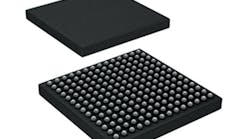
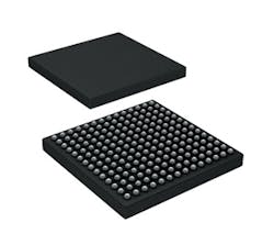
These devices come in a variety of package styles that can be sorted according to parameters, such as sampling rate and bit resolution. One recent trend common to both ADCs and DACs is to incorporate more supporting functions within each data converter circuit in ever-smaller packages and operating at lower power levels. For example, Richardson RFPD recently announced its support for Analog Devices’ AD9684 ADC. Although supplied in a compact housing (see figure), this is actually two ADCs in one package, designed for sampling wide-bandwidth analog signals.
The 14-b dual ADC operates at sampling rates to 500 Msamples/s at low power levels and with excellent linearity. The 196-ball, ball-grid-array (BGA) package, which contains an on-chip buffer and sample-and-hold circuit, measures just 12 × 12 mm. The dual ADC circuits feature a multistage, differential pipelined architecture with integrated output error-correction logic. The converter offers dual buffered inputs and an integrated voltage reference.
The AD9684 consumes only 1.1 W per channel when running at 500 Msamples/s. It achieves a full-scale SFDR of 85 dB for a 170-MHz input signal, and a full-scale SNR of 68.6 dB for the same input signal at a 500-Msample/s rate. The device well represents the trends in data converters, providing increased functionality in smaller packages and operating at lower power levels.
Higher sampling rates are also readily available. One such example is the direct-RF-sampling ADCs from Texas Instruments, which handle input signals to beyond 3 GHz at sampling rates to 4 Gsamples/s and 12-b resolution.
In effect, a wide-bandwidth, high-sampling-rate ADC can replace a portion of a radio front end. For instance, it can replace one intermediate-frequency (IF) section (and its associated components, including mixers, oscillators, and amplifiers), thus reducing circuit size and cost for the radio design. Potential savings in operating power when using this current generation of ADCs and DACs can also pay tremendous dividends for customers of portable radios and other electronic products.
This file type includes high resolution graphics and schematics when applicable.


