This file type includes high-resolution graphics and schematics when applicable.
Antennas are the beginning and end components of many communications systems, and the performance of modern wireless communications networks depends on these antennas achieving low passive-intermodulation (PIM) levels. PIM is a complex phenomenon that results in the generation of spurious energy. It is not caused by circuit materials, but results from the design and mechanical structure of high-frequency circuits, from circuit-assembly practices, and/or from system-level effects.
Still, circuit materials can play a part in achieving low PIM in PIM-sensitive applications. For low-PIM printed-circuit-board (PCB) antennas, some of the PIM performance depends on the design, and some on the choice of PCB materials. Understanding how PCB characteristics influence PIM performance can ease the task of choosing circuit materials for low-PIM PCB antennas.
Maintaining low PIM in a communications system is a complex problem due to the large number of variables that contribute to PIM. A quick list of PIM-causing variables includes cables, connectors, passive components, solder joints, and even placement of hardware. It gets even more complex with interactions among variables. The proper choice of circuit materials for a PCB antenna can at least shrink one list of variables.
Rise of PIM
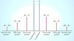
PIM has become more of a design issue in recent years with the growing number of wireless applications and their associated signals occupying a limited amount of available bandwidth. Two or more closely spaced signals within the same operating band can produce intermodulation distortion due to the mixing of their lower-order harmonics and the mixing of those harmonics with the two fundamental signals (Fig. 1). The signals may come from the same wireless base station, or they could be signals reaching the antenna from additional, outside sources.
Such intermodulation was once only associated with active devices, such as semiconductor mixers and amplifiers, but in recent years it has become evident that intermodulation can be caused by passive components, too, including antennas. It can affect applications with single antennas used for transmit and receive functions and multiple carrier frequencies, especially when those antennas exhibit the nonlinear behavior that could create PIM. When the amount of spurious energy produced as PIM falls within the operating frequency range of a receiver, it can qualify as interference.
At the system level, anything in the RF signal path between the transmitter and receiver can cause PIM, especially ferromagnetic materials or metals and any materials with ferromagnetic properties. Materials such as rust and metals like nickel and iron can be sources of PIM. Anything that interrupts the signal path of a transmission line, e.g., poorly fitted interconnections or debris in the mating area of connectors, can cause PIM. Even a rusty fence in the vicinity of a wireless transmitter could trigger PIM, with sufficiently high transmit power.
In a PCB-based antenna, such as a microstrip patch antenna, circuit cleanness (or lack thereof) may also cause problems. For example, residue remaining on a PCB following fabrication and left behind by inadequate PCB cleaning procedures can be sufficient to induce nonlinear effects that result in PIM. A number of different kinds of plated finishes on PCBs can contribute to higher levels of PIM—electroless nickel, immersion gold (ENIG), and electroless nickel, immersion palladium, immersion gold (ENIPIG) are two such types.
Material Consistency
The choice of PCB material itself may also play a part in the PIM performance of a PCB antenna. Several circuit material parameters can be used to project how well a PCB antenna is expected to perform, including consistency of dielectric constant (Dk), stability of Dk with temperature, and mechanical stability with temperature. Ideally, the Dk of a circuit substrate material should be uniform throughout each board and consistent from board to board for good circuit-to-circuit repeatability.
Because Dk determines the circuit dimensions required for optimum antenna performance at a desired wavelength/frequency, any circuit material intended for PCB antenna design should feature Dk within a tight tolerance. Although predicting PIM performance for any antenna design is difficult, using the optimum circuit material to achieve the best performance for a printed antenna will also generally deliver the best PIM performance.
In a microstrip patch antenna, for example, the patch pattern is etched to dimensions matching a specific fraction of a wavelength for the center frequency of a band of interest, such as a quarter wavelength. Since wavelength is a function of frequency, with higher frequencies yielding shorter wavelengths, printed antenna dimensions will also shrink with increasing frequencies.
The Dk determines the impedance of the patch pattern and the microstrip transmission lines feeding the patch. Consequently, excessive variations in a circuit material’s Dk will result in changes in impedance and frequency throughout the printed antenna circuit and unwanted variations in antenna radiation pattern. A Dk tolerance of ±0.05 is considered quite good for printed antennas, as well as for most other high-frequency circuit applications.
Consistent circuit material Dk is also desirable across a wide operating temperature range. That’s because printed antennas and their transceivers may be asked to perform flawlessly over a wide range of operating conditions, from day to day or from season to season in outdoor base stations and cell sites.
The parameter that provides insight into the stability of a circuit material’s Dk with temperature is the thermal coefficient of Dk (TCDk). For a given material, this parameter notes by how many parts per million (ppm) the Dk will change per change in temperature in degrees centigrade (°C). If the TCDk value of a material is high, the Dk will change by a relatively large amount with temperature, and will change the antenna’s resonant frequency as well as alter the radiation pattern for the desired frequency range. A TCDk value can be positive or negative, depending upon the formulation of the circuit material. Considering the absolute value of a material’s TCDk, a value of 50 ppm/°C or less is quite good, or within the range of ±50 ppm/°C.
In terms of real-world circuit materials used for PCB antennas, FR-4 typically represents a low-cost circuit material solution. However, the tradeoff for low cost is a Dk that varies widely with temperature, characterized by a high value of TCDk. When room temperature (or +25°C) is used as the starting point for normalized Dk, a circuit material’s Dk may increase or decrease at other temperatures. When compared to other circuit materials, the changes for FR-4 can be dramatic, with significant decreases in Dk at temperatures below +25°C and large increases in Dk for temperatures above +25°C.
Ideally, materials for PCB antennas should provide stable Dk with temperature, denoted by lower values of TCDk. Depending on formulation, commercial materials, such as RO3003 and RO4003 laminates from Rogers Corp. can have negative or positive TCDk values, describing how the material Dk changes with temperature. For RO3003 laminates, which are polyetrafluoroethylene (PTFE) circuit materials reinforced with ceramic fillers, the TCDk is extremely low and negative, at only –3 ppm/°C, for very little change in Dk with temperature. This material has a Dk of 3.00 with tolerance of ±0.04. For RO4003 laminates, which also have quite low TCDk, the value is positive at 40 ppm/°C. This hydrocarbon circuit material, reinforced with ceramic filler, has a Dk value of 3.38 and tolerance of ±0.05.
Another circuit material parameter for antennas related to temperature is coefficient of thermal expansion (CTE). Though also given in units of ppm/°C, it is a measure of the mechanical changes in a circuit material due to changes in temperature. Because a material will expand and contract according to changes in temperature in its x, y, and z axes, the CTE of candidate materials for an antenna design must be compared in all three axes.
In particular, these CTE values should be compared to the CTE values for other materials used on a PCB. This includes the copper used to form a patch antenna pattern and its microstrip feed lines, in addition to copper plating used on plated through-holes (PTHs) that might connect an antenna to the different layers of a multilayer circuit. In the x and y dimensions, the circuit patterns and the dielectric material will expand and contract; in the z dimension, the metal of the PTHs and the thickness of the dielectric material will change with temperature.
Ideally, the CTE values for all materials of interest should be fairly closely matched. This will prevent stresses at the interfaces of different materials caused by mechanical changes with temperature. Since the CTE of copper is about 17 ppm/°C, a CTE value for a PCB material that is within range of copper is considered good, such as 60 ppm/°C or less. The CTE is not just a factor to consider for printed antenna performance and reliability. It is also an indicator of a circuit material’s capability to withstand the high temperatures used when manufacturing a printed antenna, such as for lead-free solder-reflow processes.
Patrolling Antenna PIM
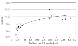
When considering high-frequency circuit materials for printed antennas, metallic rather than dielectric materials are the main concern. Rough copper-laminated surfaces of PCB materials are a leading source of PIM in such antennas. Ideally, the surface of a PCB’s copper laminate should be as smooth as possible to promote linear behavior. Specifically, the surface of concern is the copper-substrate interface of the laminate. As the roughness of the copper surface increases, the EM behavior of the copper as a conductor becomes increasingly nonlinear and more subject to generating higher levels of PIM as an antenna circuit (Fig. 2).
As noted earlier, treatments applied on the copper foil can raise a PCB antenna’s level of PIM. Treatments are often performed to improve the adhesion of the copper layer to the dielectric layer. However, a copper treatment with ferromagnetic properties such as nickel-based treatments can be a source of higher PIM levels; therefore, it’s a good idea to minimize use of such PIM-causing treatments.
In terms of a PCB’s dielectric material, for low PIM levels, the guidelines provided earlier should be followed for consistent Dk held within a tight tolerance window. In addition, the dielectric material should exhibit low loss as evidenced by a low value of dissipation factor (Df).
Furthermore, as a simple rule of thumb, a thinner circuit laminate will yield worse PIM performance than a thicker circuit laminate, although this is not due to the dielectric properties. The amount of PIM is very much subject to the design of the printed circuit. In a thinner antenna circuit, greater power density is concentrated in a smaller area than a thicker antenna circuit with wider conductors. If any conditions for PIM are present, such as rough copper foil or residue from PCB fabrication, the higher power density will add to conditions favorable for generating higher levels of PIM.
Although PIM is a type of distortion that affects system-level communications performance, it starts at the component level (i.e., connectors, antennas,etc.). As wireless communications services extend throughout the world, with strong competition for available frequency bands, PIM becomes more critical than ever. As a result, lower levels of PIM are required to maintain system-level performance and avoid symptoms such as dropped calls and diminished coverage areas.
PIM performance can be compared in terms of dBm (power relative to 1 W) or dBc (power relative to the carrier). A PIM level of –145 dBc was once considered satisfactory. But as the number of subscribers increased along with the number of cell sites to serve them, required PIM levels continued to drop. They initially fell to –150 dBc, and now –153 dBc is considered adequate.
To achieve printed antennas with the performance required for low PIM, the circuit materials must play their parts to help minimize intermodulation distortion. Although no industry-standard test methods exist for characterizing circuit materials for PIM, a technique was developed to characterize the latest generation of low-PIM circuit laminates, such as RO4730G3 circuit material from Rogers Corp. (see “Laminates Lay Foundation for 5G Antenna Circuits”).
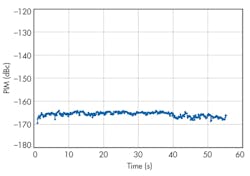
Evaluation involved the fabrication of a 12-in.-long microstrip transmission-line circuit on 60.7-mil-thick RO4730G3 laminate. Since so many variables can impact PIM and its testing, a circuit’s PIM performance may change dramatically over even the short period of time required for testing (i.e., a few seconds). To reveal consistency in PIM performance, measurements should be performed for a time period much longer than just those few seconds. Thus, the microstrip circuit’s PIM performance was measured for a total of 55 s, with 10 data points collected every second to produce a total of 550 plots of PIM versus time (Fig. 3).
The RO4730G3 material, which was engineered for printed antennas, is capable of PIM levels of –163 dBc or better. It is an example of a material with the characteristics—tight Dk tolerance, smooth copper foil, excellent CTE—that support low PIM levels for printed-circuit antennas.
Editor’s Note: To learn more about the test methods used to characterize circuit laminates for PIM, copies of “PIM and PCB Antennas: Your Guide to Circuit Materials for Low Passive Intermodulation (PIM) Antennas” are available for free download at www.rogerscorp.com.


