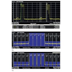
High-Speed DACs Fuel Multiband Transmitters
This file type includes high resolution graphics and schematics when applicable.
Wireless communications networks are being pushed for faster speeds and more information. Consumers are expressing increasing demands for enhanced data services, requiring wider wireless coverage and even greater use of bandwidth. Different radio technologies and increasing frequency allocations make it more complex to control networks and reduce costs. Wireless service providers are looking for solutions that not only protect their existing investments but also simplify systems for future network upgrades and capacity expansion.
Related Articles
• 25-GSamples/s DAC Powers Function Modules
• Building Base Stations For Use In Homes
• Companies Join Forces to Develop Small-Cell Base Stations
One solution is the use of multiple-frequency-band, multiple-communications-standard wireless networks, including multiband, multistandard-radio (MB-MSR) base stations. A challenge for radio designers is the cost-effective implementation of such radio base stations with current technology. Fortunately, supporting the evolution of radio base station design is the latest generation of radio-frequency digital-to-analog converters (DACs), such as the model AD9129 DAC from Analog Devices. Some of the considerations for designing an MB-MSR transmitter using RF DACs will be detailed here.
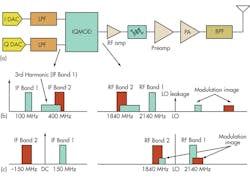
Figure 1(a) offers an example of a system architecture widely used in wireless base station transmitter design. The in-phase (I) and quadrature (Q) input data is digitally modulated and converted in the DAC to a pair of I and Q output signals at an intermediate frequency (IF). This IF should be properly selected so that it is high enough for the bandpass filter to reject the modulation image, yet low enough for the DAC to maintain good output performance. This architecture has been successfully implemented in single-band radio designs for multiple generations. The advantages and design tradeoffs are well known. However, there are a few inherent limitations associated with this architecture that would make it more difficult to plan the frequencies in a multiband radio design.
Figure 1(b) illustrates one of the limitations often encountered when directly applying this architecture to a multiband design. In a single-band radio, the harmonics of the signal at the DAC output are typically treated as out-of-band spurious signals and rejected by the lowpass filter following the DAC. In the dual-band application, these harmonic signals may fall in-band and within the higher transmit band. This limitation is avoided in the approach shown in Fig. 1(c). The two signal bands are placed centered around DC in the complex domain. The harmonic signals then appear out of band and can be removed by filtering. This approach also has a lower requirement for the DAC sample rate and lowpass filter bandwidth due to its narrower real signal bandwidth.
Nevertheless, a problem with this frequency plan occurs at the modulator output. Depending on the distance of each band from the local-oscillator (LO) frequency, the modulation image of each signal tends to fall in the vicinity of the other band. Although it is possible that a sophisticated quadrature error correction (QEC) algorithm can help suppress the images, it may place an extra burden on the baseband signal processing engine because analog filtering techniques are not available when the images are in band.
From an architecture perspective, the DAC plays a critical role in a radio transmission system. Its speed and performance determine how physically close to the antenna digital-to-analog conversion can be performed. The RF DAC extends the scope of digital signal processing beyond the baseband domain to the antenna. It enables synthesis of the baseband digital signal directly at the final output frequency, which essentially absorbs the analog upconversion operation of the traditional architecture into the digital domain. Digital frequency conversion provides greater flexibility and higher performance in terms of frequency planning and noise. This is especially attractive to the MB-MSR design.
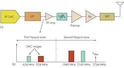
The frequency planning is more flexible using the RF DAC because the digital modulation is ideal and does not generate modulation images that can interfere with signals. The DAC sample clock frequency is the only design variable that needs to be determined in the frequency planning. Figure 2 shows the architecture of direct RF synthesis with an RF DAC and its capability of supporting dual-band applications without having issues in the traditional architecture. In this example, the dual-band signal is directly synthesized at the final transmission band frequencies. The DAC sample clock frequency is chosen so that the harmonics of the signals fall far out of the band of interest and can be filtered before the signal is fed into the next RF stage.
The noise performance in the direct-to-RF architecture is better for two reasons. The first is elimination of the analog upconversion stage. In traditional architectures, the overall noise figure of the transmit signal chain is typically dominated by the modulator noise since the noise contributed by the DAC at the modulator output is usually lower than the modulator’s output referred noise floor. Removing the modulation stage allows the system designer to lower the system noise figure by taking advantage of the DAC’s low noise floor and the high gain of the RF amplifier. The second reason for better noise floor is reduction of the insertion loss for the antenna when transmitting in multiple bands since no combiner is needed. The RF DAC’s capability to synthesize multiple bands thus improves the overall performance of the system, in addition to reducing complexity (and therefore, size and cost).
Typical multiband communication systems include data interface logic; a field programmable gate array (FPGA) or specialized application-specific integrated circuit (ASIC); DACs; filters; gain blocks; and RF power amplifiers. Within a channel card, the DAC acts as the interface between the digital logic and the RF analog output driving network. The DAC plays an important role in the system as its performance, sample rate, and bandwidth all influence the system architecture and design. Some key circuits—such as the DAC output path, clock circuit, transmission lines, power supply, and return paths—need particular attention to ensure their designs are correct for optimal performance. Analysis and simulation of these blocks, as well as the DAC printed-circuit board (PCB), may be needed.
Power Considerations
In addition, power supply routing can be challenging. The digital logic includes input/output (I/O) and core logic power supplies, while the RF output network can include as many as four or five additional power supplies. The power domains must be isolated from one another and signal return paths need to be carefully managed to ensure no crosstalk between supply domains. Keeping the power supplies isolated from one another is crucial to low noise performance.
Related Articles
• 25-GSamples/s DAC Powers Function Modules
• Building Base Stations For Use In Homes
• Companies Join Forces to Develop Small-Cell Base Stations
The main DAC clock is one of the most critical signals on the system card. The DAC clock is a differential signal and is isolated from other signals with via fences. In addition, return paths are controlled to ensure no coupling or crosstalk. Any signals coupling onto the clock will directly appear at the output of the DAC. Digital signals corrupting the clock reduce the noise margin in the system. Even the DAC outputs must be prevented from coupling onto the clock, as this will cause second harmonics and potentially higher-order harmonics to appear in the output spectrum.
It is preferable to keep the clock driver as close as possible to the DAC to reduce noise and other coupling concerns. The DAC outputs are connected to their load by transmission lines. The impedance of these transmission lines is carefully controlled to the load to ensure predictable behavior of the DAC output signals. The RF DAC’s output impedance is related to the package as well as the die, so the laminate’s effects must be included in analysis and simulation of the output stage. Matched impedance between the DAC and the load is critical to maximize the power transfer from the DAC to the destination, and also to minimize reflection from the destination back to the DAC. Proper transmission line design improves the signal-to-noise ratio (SNR), which is necessary for a good multiband communication system.
Today, typical multiband communication systems include multiple RF chains that consist of IF DACs, quadrature modulators, bandpass filters, RF power amplifiers and a final filter stage before the antenna. This architecture requires significant board space to fit multiple frequency bands into a single transmitter. This large number of components draws significant amounts of power and generates a fair amount of heat that requires removal via a heat sink or a fan, which adds complexity and cost to the overall system design.
Since RF DACs have enough bandwidth to synthesize multiple RF bands, they can be used to create a single transmitter with a multiple-band output. For example, a triple-band transmitter that may require three pairs of IF DACs, three modulators, and three bandpass filters may be replaced by a single RF DAC and output filter that generate all three bands. As power amplifier designs migrate to wider bandwidths, even greater savings of circuit-board space can be realized as the number of components in distinct RF chains is reduced to those needed only after the power amplifier. Thus, a multiple-band transmitter could be implemented with an RF DAC, an output filter between the DAC and power amplifier, a power amplifier, and output filters between the power amplifier and the antenna.
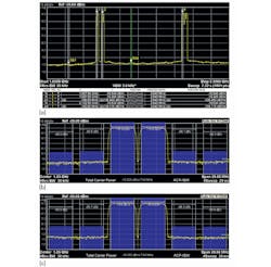
Figure 3 shows the output of the AD9129 RF DAC at a sample rate of 2764.8 MSamples/s using a selectable mode in the DAC that enables use of the second Nyquist zone. It is a 14-b DAC readily capable of operating at sampling rates to 2.8 GSamples/s and beyond. Eight 5-MHz-wide wideband-code-division-multiple-access (WCDMA) channels were synthesized at three different bands. Two channels were created from 1825 to 1835 MHz, two other channels at 1845 to 1855 MHz, and four channels at 2130 to 2150 MHz. The signals were generated in a field-programmable gate array (FPGA) and then directly synthesized by the RF DAC.
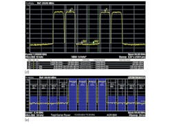
Figure 4 shows the output of the AD9129 at a sample rate of 2764.8 MSamples/s using a mode that enables synthesis in the first Nyquist zone. Four 5-MHz-wide WCDMA channels with four Long-Term-Evolution (LTE) downstream channels were synthesized at two different bands. Four WCDMA channels at 871 to 891 MHz, and four LTE downstream channels were created at 729 to 749 MHz.
Modern wireless communication networks demand for flexible, easy-to-upgrade multiband, multistandard base stations. The direct-to-RF transmitter architecture provides a cost/performance effective solution for the multi-band, multi-standard radio transmitter design. The advancement of the RF DAC technology, such as the AD9129 from Analog Devices, has helped lower the threshold of a multi-band and multi-standard radio design and has shown a promising trend of having more designs using the direct-to-RF architecture in the future.
Yi Zhang, HCG Application Engineer
Assaf Toledano, HCG Product Engineer
Analog Devices, Inc., One Technology Way, Norwood, MA 02062-9106; (800) 262-5643, (781) 329-4700.
This file type includes high resolution graphics and schematics when applicable.


