Low-Cost Front End Receives 9 GHz
This file type includes high resolution graphics and schematics when applicable.
Increasing use of wireless systems and their services is continuing to drive data rates and consume available bandwidths. In recognition of this, the Radiocommunications Sector of the International Telecommunication Union (ITU-R) has established wireless data rates to 100 Mb/s for high-mobility applications and 1 Gb/s for low-mobility applications1 through its IMT-Advanced standards. The ITU recognizes the need to support wireless data rates to 10 Gb/s and beyond.
These higher data rates will require greater spectrum resources and a push to higher frequencies, such as the use of the 3.5-GHz band for the Time-Division, Long-Term-Evolution (TD-LTE) system detailed in ref. 2. Therefore, lowering the complexity and cost of a wireless transceiver’s front end is vital in implementing mobile communication systems for these higher-frequency bands. As an example, ref. 3 details a receiver in the 6.1-GHz band with 100-MHz bandwidth designed to support 1-Gb/s wireless service. For systems operating beyond IMT bands, even wider channel bandwidths will be required.4,5
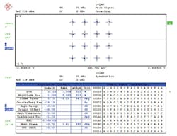
To support higher-frequency wireless applications, a wideband superheterodyne receiver was designed for X-band use at 9 GHz. The front end, which employs a commercial mixer and GaAs high-electron-mobility-transistor (HEMT) amplifiers, can be fabricated with standard printed-circuit-board (PCB) techniques and low-cost PCB laminates. It translates RF input signals to a 2-GHz intermediate-frequency (IF) band and provides a 200-MHz bandwidth at 9 GHz, with better than 3.5-dB noise figure and input return loss of better than 19 dB. The conversion gain is better than 35 dB, with gain ripple of a mere 1.24 dB. For high-speed mobile applications that require good error-vector-magnitude (EVM) performance, the front end also meets the EVM performance requirements of those systems.
As shown in Fig. 1, the receiver front end is composed of six parts, including a low-noise amplifier (LNA) RF and IF filters, and a local-oscillator (LO) module. A commercial mixer is used for frequency downconversion (from 9 to 2 GHz), while a two-stage gain block is used as the IF amplifier to guarantee link gain.
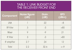
According to system requirements, the overall conversion gain of the receiver front end should be greater than 30 dB and the input 1-dB compression point higher than -30 dBm. With the help of the Advanced Design System (ADS) simulation software from Agilent Technologies, the link budget of the receiver front end was simulated and optimized. Table 1 shows the final gain distribution of the RF and IF modules.
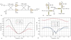
Figure 2(b) shows the circuit topology of a single amplifier (LNA1, LNA2, and LNA3). Since the HEMT tube is conditionally stable over the frequency band of interest, a small resistance is added behind it to improve stability. A bandstop filter with quarter-wavelength microstrip line and open-circuit sector stub is designed in a bias network to choke off RF transmission over its stopband, all the while maintaining optimum transmission characteristics for direct current.7,8
In simulations of the two-stage LNA using ADS simulation software, the LNA design yielded a simulated noise figure of less than 0.7 dB, with |S21| of greater than 27 dB, and |S11| and |S22| of less than -20 dB from 8.8 to 9.2 GHz.
This file type includes high resolution graphics and schematics when applicable.
Filtering Considerations
This file type includes high resolution graphics and schematics when applicable.
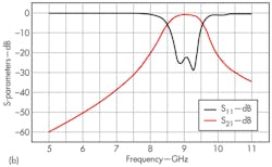
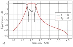
Channel filtering for the receiver front end is performed in the IF blocks by means of passive filters with high selectivity.9 To prevent possible image-signal interference of desired signals, and to keep unwanted signals from jamming the receiver front end, an RF image-rejection filter is needed in the front end. A microstrip interdigital filter was adopted in this design due to advantages of simple structure, easy implementation, compact size, and low cost. Figure 3(a) shows the layout of the designed microstrip interdigital bandpass filter. Simulated responses for the filter design were obtained by means of ADS Momentum software simulation, and are plotted in Figs. 3(b) and (c).
As shown in Fig. 3(a), the bandpass filter consists of an array of quasi-TEM-mode transmission-line resonators, each of which has an electrical length of 90 deg. at the midband frequency and short-circuited at one end while open-circuited at the other end with alternative orientation. Tapped lines with a characteristic admittance equal to the source/load characteristic admittance are used for the filter’s input and output ports.8 The position of the input/output tapped line affects the filter’s matching.
The center frequency depends on lengths l1 and l2. Coupling is achieved by the fields fringing between adjacent resonators separated by spacings s1 and s2. Coupling grows stronger with narrower spacings, and the bandwidth increases. Spacings s1 and s2 have great influence on matching, so there are tradeoffs between the bandwidth and the reflection coefficient during the design process. As Figs. 3(b) and (c) show, the filters achieve excellent performance. The dimensions are detailed in Table 2.
The performance of the LO module is important to the receiver front end. The LO module (Fig. 4) is composed of a frequency synthesizer integrated with a low-noise digital phase frequency detector (PFD) and a precision charge pump (CP), a passive third-order loop filter, and a voltage-controlled-oscillator (VCO) chip. The VCO provides the required frequency band and low-noise characteristics. A 10-MHz reference signal was provided to the LO module by a model SMF100A signal generator from Rohde & Schwarz, which was part of the test system. The phase-locked loop (PLL) for the receiver front end is designed for an output center frequency of 7 GHz. To ensure adequate LO signal power, an amplifier was added.
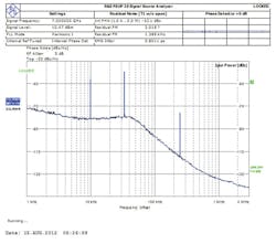
To maintain reliable high-speed digital wireless communications, LO phase noise should be minimized. Within the PLL’s loop bandwidth, the PLL phase detector is typically the dominant noise source; outside the loop bandwidth, the VCO noise is often the dominate noise source.10 Therefore, the loop bandwidth is optimized to improve the phase-noise performance. Figure 5 shows the measured phase-noise performance of the PLL used in the receiver front end. The phase noise is better than -70 dBc/Hz offset 1 kHz from the carrier, better than -80 dBc/Hz offset 10 kHz from the carrier, and better than -90 dBc/Hz offset 100 kHz from the carrier.
This file type includes high resolution graphics and schematics when applicable.
Test Results
This file type includes high resolution graphics and schematics when applicable.
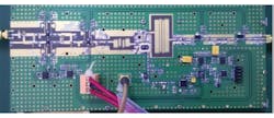
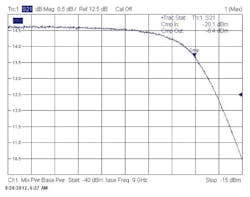
The RF receiver front end was fabricated using a standard PCB process (Fig. 6) and was evaluated with the aid of commercial test equipment. The measurement system included a model SMF100A signal generator, a model ZVA40 vector network analyzer (VNA), a model FSUP signal source analyzer, and a model FSQ signal analyzer, all from Rohde & Schwarz, and a model E8267D signal generator with option H44 from Agilent Technologies. Measurements were made of a variety of performance parameters, including gain, gain flatness, input VSWR, noise figure, image rejection, and input 1-dB compression point, with summaries presented in Table 3. The input 1-dB compression point for the entire system was measured at -20.1 dBm, as shown in Fig. 7 (a 20-dB attenuator was added at the IF port of the RF front end during the test to protect the input port of the model ZVA40 VNA).
As these results reveal, the receiver front end is well suited for mobile communications within this higher-frequency band. In addition, due to its extremely low cost, the proposed front end is suitable for large-scale applications, such as in multiple-input, multiple-output (MIMO) systems.
Acknowledgments
This work was supported in part by the National Natural Science Foundation of China under Grant No. 60702163, and in part by the National Science and Technology Major Project of China under Grant Nos. 2010ZX03007-002-01 and 2011ZX03004-003.
Lina Cao, Master’s Candidate
State Key Laboratory of Millimeter Waves, Southeast University, Nanjing, Jiangsu, 211111, People’s Republic of China; +86-15850608372
Jianyi Zhou, Professor
State Key Laboratory of Millimeter Waves, Southeast University, Nanjing, Jiangsu, 211111, People’s Republic of China; +86-025-52091653-401
Dahai Ni, Master’s Candidate
State Key Laboratory of Millimeter Waves, Southeast University, Nanjing, Jiangsu, 211111, People’s Republic of China; +86-15151859518
Shun Zhao, Master’s Candidate
State Key Laboratory of Millimeter Waves, Southeast University, Nanjing, Jiangsu, 211111, People’s Republic of China; +86-15850670606
This file type includes high resolution graphics and schematics when applicable.
References
This file type includes high resolution graphics and schematics when applicable.
1. A. Hashimoto, H. Yoshino, and H. Atarashi, “Roadmap of IMT advanced development,” IEEE Microwave Magazine, Vol. 9, 2008, pp. 80-88.
2. Lianqing Ji, Jianyi Zhou, Ke Zhou, and Jianfeng Zhai, “Design of Compact MIMO Transceivers for TD-LTE Base Station,” unpublished.
3. Zhiqiang Yu, Jianyi Zhou, Li Zhao, and Linlin Dai, “The Design of a 6-GHz Band RF Receiver with Excellent I/Q Image Suppression,” in ICMMT, May 2012, pp. 1-4.
4. Zhiqiang Yu, Jianyi Zhou, Jianing Zhao, and Wei Hong, “Design of a Wideband RF Receiver for the Next-Generation Wireless Communication System,” in Proceedings of the Asia-Pacific Microwave Conference (APMC) 2009, December 2009, pp. 465-468.
Related Articles
• RF Front End Is Reconfigurable
• Process Technology To Cut Mobile Device Front-End Size
• RF Front-End Market Will Double by 2018
5. Ke Zhou, Jianyi Zhou, and Zhiming Xu, “Design of a High Performance transceiver for TDD-LTE system,” in Proceedings of the 2012 IEEE MTT-S, June 2012, pp. 1-3.
6. Li Zhao, Zhiqiang Yu, and Jianyi Zhou, “Design of an Ultra Low Noise Amplifier For Mobile Communication in Higher Frequency Band,” in ICMMT 2010, May 2010, pp. 656-659.
7. Fei Zhou, Zhiqiang Yu, and Jianyi Zhou, “A High Performance RF Transmitter for Mobile Communication System in High Frequency Band,” in ISSSE 2010, September 2010, pp. 1-4.
8. Jia-Sheng Hong and M.J. Lancaster, “Microstrip Filters for RF/Microwave Applications,” Wiley, Hoboken, NJ.
9. Qizheng Gu. “RF System Design of Transceivers for Wireless Communications,” Nokia Mobile Phones.
10. Dean Banerjee, “PLL Performance, Simulation and Design Handbook”, 4th ed., National Semiconductor, Sunnyvale, CA.
This file type includes high resolution graphics and schematics when applicable.


