This file type includes high resolution graphics and schematics when applicable.
Mixer linearity is critical to modern communications systems, especially for ultrawideband (UWB) applications, but requires imaginative circuit-design approaches. One novel double-balanced-mixer circuit employs a source degeneration common-source topology where four tail current sources are used as degeneration resistors to improve circuit linearity. To minimize power consumption while operating on a low supply voltage, bulk-injection and forward-body-bias techniques are also employed in this design.
This double-balanced mixer covers 1.5 to 11.5 GHz with conversion gain of 6.0 to 7.2 dB. It achieves single-sideband (SSB) noise figure of 18.4 to 20.5 dB with an input third-order intercept (IIP3) of about +1.0 to +6.84 dBm , at the same time consuming only 0.46 mW power from a +0.75-VDC supply voltage.
Increasing demand for low-cost, high-performance portable wireless communications has triggered intensive research on CMOS radio-frequency (RF) front-end circuits. It is well-know that with continuous shrinking of the feature sizes in CMOS devices there is a proportional downscaling in the supply voltage; this yields superior active device high-frequency characteristics in term of power consumption, operating speed, and area.1 However, power consumption remains an issue due to limited battery capacity. Consequently, design for low-voltage and low-power radio-frequency integrated circuits (RFICs) have attracted significant attention and numerous advanced circuit techniques have been proposed in the past few years.2-11
Being widely used in wireless transceivers, the mixer is a crucial component that performs frequency conversion. The conventional Gilbert-type mixer provides high-conversion-gain (CG), low-even-order distortion with superior port-to-port isolation, and is thus beneficial for integrated-circuit (IC) applications. However, due to three-level transistor stacking, the supply voltage available to an active mixer is relatively high. Thus, an IC mixer is inevitably constrained by power consumption.
To satisfy the requirements for low-power operation while maintaining acceptable circuit performance, various design strategies and circuit techniques have been proposed in references 12 through 19. A low-voltage architecture using inductor-capacitor (LC) tanks was adopted in ref. 12. Since the LC tanks require no voltage headroom, this approach allows for a relatively large output swing. Unfortunately, the low Q-value of the spiral inductor limits the operation frequency while still occupying a large die size.
A transformer-based architecture was employed for low power in ref. 13, but the transformer imposed a narrow bandwidth limitation. Another modified mixer structure based on a Gilbert-cell topology was reported in ref. 14, where the mixer core design uses PMOS transistor stacking on the NMOS transistor. However, due to the poor performance of PMOS transistors at high frequency, the operating frequency was limited and the supply voltage was still high. This design was deemed unsuitable for low-power and low-voltage applications.
In order to alleviate the limitations imposed on the supply voltage, a folded-switch topology is proposed to reduce the supply voltage without deteriorating other design parameter.15,16 Nevertheless, the DC current between the transconductance and commutating stages is split—not reused—and may consume an increased power consumption even with a reduced supply voltage.
On the other hand, ref. 17 employs a complementary current-reuse topology with a current-bleeding technique to reduce power consumption. This design approach provides the benefit of reusing DC biasing current and reducing the bias current through the IF and switching stages. However, it suffers from relatively low gain and is usually limited to narrowband operation. Passive mixers offer high linearity and low noise figure with little DC power dissipation,18,19 but they have high conversion loss and also limited isolation between the RF and LO ports. Moreover, large LO signals required to drive passive mixers can significantly increase the power consumption of a receiver system.
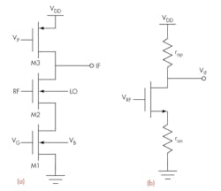
What follows is a qualitative description of the mixer’s core operation followed by a detailed look at its performance. Figure 1(a) shows the schematic diagram of the mixer core, which consists of a current source stage (M1), a bulk-driven stage (M2), and a PMOS transistor (M3) as an active load. In contrast to a Gilbert-type mixer, the bulk-injection mixer is based on a four-terminal device where the RF and local-oscillation (LO) signals are applied to the gate and bulk of transistor M2, and the intermediate-frequency (IF) signal is pumped from the drain.20 As a result, the proposed mixer can operate at a reduced supply voltage due to its one less stacked stage compared with a Gilbert-type mixer.
This file type includes high resolution graphics and schematics when applicable.
Manipulating The Threshold Signal
This file type includes high resolution graphics and schematics when applicable.
In addition, owing to the bulk-injection technique, the parasitic capacitance between the RF and LO stages—which significantly degrades the conversion gain at a high frequency—is eliminated without a matching LC network. Therefore, a widely flat conversion gain can be achieved across the entire bandwidth. Since the LO signal is injected into the bulk of the core transistor M2, the threshold voltage can be manipulated by the LO signal at the body terminal. Typically the threshold voltage of an n-channel MOSFET is given by Eq. 121:
VTH (LO) = VTO + r([2|φF| - VBS(LO)]0.5 - [2|φF|]0.5 (1)
where:
VBS = the source-to-bulk potential difference;
VTO = the threshold voltage for VBS = 0;
r = the body-effect coefficient; and
φF = the Fermi potential with a typical value in the range of 0.3 to 0.4 VDC.22
From Eq. 1, it can be seen that the threshold voltage VTH (LO) of the transistor is a function of the voltage between the bulk and source, VBS, and the device M2 is switched on and off alternately as the LO signal is in the positive or negative phase of the LO. Hence, the mixing function is achieved by the LO signal, which modulates the threshold voltage of transistor M2.
On the other hand, the mixer core is similar to a common-source degeneration structure in a low-noise amplifier (LNA), where transistor M1 not only acts as the tail current source but also as a degeneration resistor to improve the linearity of the mixer. The high output impedance of PMOS transistor M3 is used as an active load to transfer current to voltage for the IF output signal. Moreover, the forward bias voltage VB is employed at the body of M1 to meet the low-voltage-supply design.
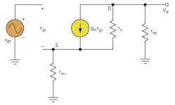
To suppress the noise influence of the following blocks and reduce the requirement for the gain of LNA, the UWB mixer should exhibit reasonable conversion gain. Based on the schematic diagram of Fig. 1(b), Fig. 2 shows the small-signal equivalent circuit of the bulk-injection mixer core. Assuming that the gate-drain parasitic capacitance, Cgd, along with body effects are ignored, the small-signal voltage gain, AV, can be solved by means of Eq. 2:
AV =vIF/vRF= -(gm/rop)/[1 + (rop/ r0) + (ron/ r0) + gm ron] (2)
where:
r0 = the channel resistance;
ron = the output resistance of transistor M1; and
rop = the output resistance of transistor M3;
gm = the transconductance of NMOS transistor M2.
Assuming that the local oscillator (LO) signal is an ideal square wave, and the RF signal is mixed with the LO signal and modulated as the desired output frequency, fRF - fLO, where fRF and fLO represent the RF and LO frequencies, the proposed mixer’s conversion gain (CG) can be expressed as Eq. 3:
CG = (-2/π) {gm rop/[1 + (rop/ r0) + (ron/ r0) + gm ron]} (3)
In practical circuit design, r0 ≈ ron, gmron ≈ 1 + rop/r0, and the expression for conversion gain can be simplified as Eq. 4:
CG ≈ (2/π)(rop/ron) (4)
From Eq. 4, it can be seen that the conversion gain of the mixer is determined solely by the output resistance of transistors M1 and M3. To achieve high conversion gain with minimum power consumption, the small-gate-width size device M3 is selected to increase the output resistance, and it also should be biased in its active region. This suggests that increases in resistance rop will boost CG to an arbitrarily high value, which is not correct. Since the voltage drop across the active load M3 is proportional to the output resistance, a large value of rop results in a low voltage between the drain and source of bulk-driven stage M2.
The above-assumed condition no longer holds as it is indicated in Eq. 4 when the low output resistance, r0, of transistor M2 is considered, which degrades the conversion gain of the mixer. Another approach for optimum conversion gain is to reduce the output resistance of M1, but at a cost of circuit linearity and power consumption. Therefore, a design tradeoff exists between conversion gain and linearity for the proposed mixer topology.
A mixer must have acceptable linearity to suppress interference and maintain high sensitivity. In a multiple-standard wideband receiver, in-band and out-of-band interference signals can result in severe blocking, cross-modulation, and intermodulation—all challenging to the linearity of the mixer. For low-power applications, a major design challenge is to achieve the required circuit linearity under limited bias conditions. A number of approaches are available for realizing a high-linearity mixer, but limited power schemes discourage additional active circuit implementations.
The post-distortion technique is one such approach available to Gilbert-type mixers.23 The quest to realize high linearity with little DC current consumption has motivated the source degeneration common-source configuration shown in Fig. 1(a). The linearity of this approach can be understood by means of a mathematical analysis, assuming that bulk-injection stage M2 is operated in its active region as it is turned on. Equate current flow through device M2 and rop in Fig. 1(b):
(VDD – vIF)/rop = βn {VG + vRF - [(VDD - vIF)/rop]ron - VTH}2 (5)
βn = (1/2)μnCox(W/L)2 (6)
where:
βn = the transconductance parameter and Cox = the gate oxide capacitance per unit area.
As indicated in ref. 14, the IIP3 can be expressed as:
IIP3 (dBm) = 10log(8c) (7)
c ≈ (1/2βn2)[4βn(VG - vTH)]2 x [{4βn(VG - VTH)ron + 1}0.5 + 1] (8)
This file type includes high resolution graphics and schematics when applicable.
Conversion Gain/Power Consumption Tradeoff
This file type includes high resolution graphics and schematics when applicable.
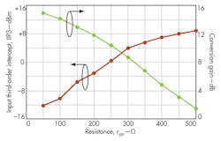
Based on Eqs. 7 and 8, it is clear that mixer linearity increases with the output resistance, ron, of transistor M1. However, mixer conversion gain is degraded as depicted by Eq. 4. Hence, a tradeoff between conversion gain and DC power consumption should be reached to achieve relatively high linearity. Figure 3 shows how simulated circuit linearity and conversion gain vary with the value of ron. For this mixer design, the output resistance values of transistors M1 and M2 are 325 and 920 Ω, respectively.
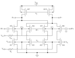
Figure 4 shows a complete circuit diagram for the low-power CMOS downconversion mixer. A double-balanced mixer configuration was chosen for enhanced port-to-port isolation. The proposed mixer consists of three parts: a current source stage (M1 through M4), a bulk-driven stage (M5 through M8), and PMOS transistors (M9 and M10) as active loads. In contrast to the cascade structure of a conventional Gilbert-cell mixer, the four bottom NMOS transistors (M1 through M4) are used as degeneration resistors to improve circuit linearity.
Meanwhile, a bulk-driven technique is employed for a low supply voltage as presented previously. In addition, a forward body bias technique is introduced to further alleviate the voltage headroom limitation imposed by the use of a low supply voltage. Since a forward body bias voltage (VLO and VB) effectively lowers the threshold voltage, this technique provides the benefit of reducing the operated voltage as well as LO power without compromising device characteristics in term of gain, linearity, and noise figure.
Moreover, current-limiting resistors RB and RLO must be employed at the body terminal to restrict the excessive junction leakage current. Voltages VG and VP represent the gate bias voltage. On-chip capacitors (C1-C2) are applied as DC-blocking capacitors to isolate the input from the DC source. To achieve low-power operation, the three stacked layers of devices are biased in the linearity, subthreshold, and active regions from the bottom up, consuming only about 0.6 mA DC current from a +0.75-VDC supply.
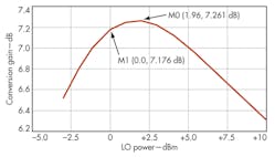
The mixer was computer simulated with SpectreRF software from Cadence Design Systems based on chartered 0.18-μm CMOS technology. By employing forward body bias and bulk-injection techniques, the supply voltage falls to +0.75 VDC. The mixer is designed to operate between 1.5 and 11.5 GHz with local oscillator (LO) power of 0 dBm. With an RF input at 5.2 GHz and LO frequency of 5.1 GHz, the simulated downconversion gain versus LO power indicates peak gain of 7.26 dB at LO power levels between 0 and +4 dBm (Fig. 5). The value of 0 dBm was chosen for LO power where conversion gain of 7.176 dB was obtained for the tradeoff between LO power and conversion gain—of particular significance to this low-power design.
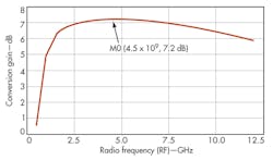
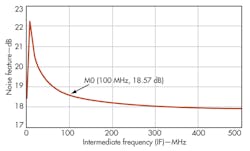
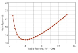
Figure 6 illustrates conversion gain over a wide RF input frequency range, with conversion gain of 6.0 to 7.2 dB from 1.5 to 11.5 GHz. Figures 7 and 8 show mixer-noise figure performance. Apart from the IF at 100 MHz, the noise figure versus IF is relatively flat, with less than 1-dB variation from 60 to 500 MHz (Fig. 7). Referring to Fig.8, the simulated single-sideband noise figure ranges from 18.4 to 20.5 dB for an RF range from 1.5 to 11.5 GHz at an IF of 100 MHz. The mixer’s relatively large noise figure is due to use of four tail current sources (M1-M4) at the bottom of mixer.
This file type includes high resolution graphics and schematics when applicable.
Summing Up
This file type includes high resolution graphics and schematics when applicable.
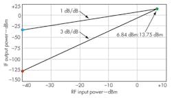
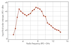
Figures 9 and 10 provide simulation results of the mixer’s input third-order-intercept-point (IIP3) performance. At a RF of 7.5 GHz, two-tone signals with a frequency spacing of 10 MHz and equal power levels of -30 dBm are applied to the downconversion mixer, with a maximum IIP3 of +6.84 dBm (per Fig. 7). With 0-dBm fixed LO power, the measured IIP3 varies from +1.0 to +6.84 dBm when the RF rises from 1.5 to 11.5 GHz (Fig. 10). The power dissipation is 0.46 mW at a +0.75-VDC supply voltage.
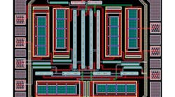
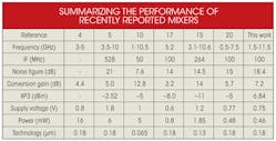
Figure 11 shows a layout for the downconversion mixer, which occupies a chip area of only 0.36 x 0.32 mm2. The table offers a comparison of the mixer’s performance with recently published results. The new mixer structure provides respectable linearity, conversion gain, and acceptable noise performance with low LO power and less power dissipation compared to other recent mixer designs.
By employing bulk-injection and forward-body-bias techniques, the CMOS downconversion mixer achieves low power consumption at low supply voltage with flat conversion gain from 1.5 to 11.5 GHz. Based on a conventional Gilbert-type approach, the mixer’s new source degeneration common-source topology using four tail current sources as degeneration resistors to improve circuit linearity. Suitable for UWB applications, it exhibits maximum conversion gain of 7.2 dB with SSB noise figure of 18.4 dB and IIP3 of +6.84 dBm while consuming only 0.46 mW power from a +0.75-VDC supply.
Kehao Ma, Master’s Candidate
Chunhua Wang, Professor and Doctoral Supervisor
Xiaorong Guo, Professor and Master’s Supervisor
Wenbin Huang, Student
Hunan University, Changsha, 410082, People’s Republic of China.
Acknowledgments
This work was supported in part by the Open Fund Project of Key Laboratory in Hunan University (No. 12K012). The authors would like to thank the anonymous reviewers for their valuable suggestions, which helped improve the quality of the article.
This file type includes high resolution graphics and schematics when applicable.
References
This file type includes high resolution graphics and schematics when applicable.
1. Henk M.J. Boots, Gerben Doornbos, and Anco Heringa, “Scaling of characteristic frequencies in RF CMOS,” IEEE Transactions on Electron Devices, Vol. 51, No. 12, December 2004, pp. 2102-2108.
2. Yong-Il Kwon, Sang-Gyu Park, Ta-Joon Park, Koon-Shik Cho, and Hai-Young Lee, “An Ultra Low-Power CMOS Transceiver Using Various Low-Power Techniques for LR-WPAN Application,” IEEE Transactions on Circuits and Systems-I: Regular Papers, Vol. 59, No. 2, February 2012, pp. 324-336.
3. I. Nam, K. Choi, J.H. Lee, H.K. Cha, B.I. Seo, K. Kwon, and K. Lee, “A 2.4-GHz low-power low-IF receiver and direct-conversion transmitter in 0.18-μm CMOS for IEEE 802.15.4 WPAN applications,” IEEE Transactions on Microwave Theory and Techniques, Vol. 55, No. 4, April 2007, pp. 682–689.
4. Lai, J.-T., Y.-S. Lin, C.-L. Lu, and H.-R. Chuang, “A 3-5-GHz, low-voltage, high-isolation transformer-based CMOS mixer for UWB applications,” Proceedings of the 3rd International Conference on Innovative Computing Information and Control, June 2008, pp. 238-241.
5. Sandhya Samadhiya and Rajesh Khatri, “Design and Analysis of Low-power, Low voltage, 3.5-10-GHz Folded Gilbert-cell Mixer for UWB Application,” 2011 International Conference on Multimedia, Signal Processing and Communication Technologies, 2011, pp. 204-207.
6. Hung-Che Wei, Chih-Lung Hsiao, and Ro-Min Weng, “A broadband low power high isolation double-balanced subharmonic mixer for 4G applications,” Progress In Electromagnetics Research, Vol. 138, 2013, pp. 143-155.
7. Hsieh-Hung Hsieh, Huan-Sheng Chen, et al., “Experimental 5-GHz RF Frontends for Ultra-Low-Voltage and Ultra-Low-Power Operations,” IEEE Transactions on VLSI Systems, Vol. 19, No. 4, April 2011, pp. 705-709.
8. H.C. Wei, R.M. Weng, and S.Y. Li, “A broadband high linearity and isolation down-conversion mixer for WiMAX applications,” Journal of Electromagnetic Waves and Applications, Vol. 23, Nos. 11-12, 2009, pp. 1555-1565.
9. Shan He and Carlos E. Saavedra, “An Ultra-Low-Voltage and Low-Powerx2 Subharmonic Downconverter Mixer,” IEEE Transactions on Microwave Theory and Techniques, Vol. 60, No. 2, February 2012.
10. S.K. Hampel, O. Schmitz, M. Tiebout, and I. Rolfes, “Inductorless low-voltage and low-power wideband mixer for multistandard receivers,” IEEE Transactions on Microwave Theory and Techniques, Vol. 58, No. 5, 2010, pp. 1384-1390.
11. Hwann-Kaeo Chiou and Hung-Ting Chou, “A 0.4 V Microwatt Power Consumption Current-Reused Up-Conversion Mixer,” IEEE Microwave and Wireless Components Letters, Vol. 23, No. 1, January 2013.
12. C.-C. Tang, W.-S. Lu, L.-D. Van, and W.-S. Feng, “A 2.4-GHz CMOS down-conversion doubly balanced mixer with low supply voltage,” in Proceedings of the IEEE Interational Symposium on Circuits & Systems (ISCAS), Vol. 4, May 2001, pp. 794-797.
13. C. Hermann, M. Tiebout, and H. Klar, “A 0.6-V 1.6-mW transformer-based 2.5-GHz downconversion mixer with +5.4-dB gain and -2.8-dBm IIP3 in 0.13-μm CMOS,” IEEE Transactions on Microwave Theory and Techniques, Vol. 53, No. 2, February 2005, pp. 488-495.
14. L. Liu and Z. Wang, “Analysis and design of a low-voltage RF CMOS mixer,” IEEE Transactions on Circuits & Systems II, Vol. 53, No. 3, March 2006, pp. 212-216.
15. J.-B. Seo, J.-H. Kim, H. Sun, and T.-Y. Yun, “A low-power and high-gain mixer for UWB systems,” IEEE Microwave and Wireless Components Letters, Vol. 18, No. 12, December 2008, pp. 803-805.
16. F.-C. Chang, P.-C. Huang, S.-F. Chao, and H. Wang, “A low power folded mixer for UWB systems applications in 0.18-μm CMOS technology,” IEEE Microwave and Wireless Components Letters, Vol. 17, No. 5, May 2007, pp. 367-369.
17. H.-H. Hsieh and L.-H. Lu, “Design of ultra-low-voltage RF frontends with complementary current-reused architectures,” IEEE Transactions on Microwave Theory and Techniques, Vol. 55, No. 7, July 2007, pp. 1445-1458.
Related Articles
• 2013 IEDM Surveys Device Developments
• Testing Automotive Radar Brings mm-Wave Challenges
• Beyond CMOS Vs. GaAs: Picking The Right Technology
18. H. Khatri, P.S. Gudem, and L.E. Larson, “Distortion in current commutating passive CMOS downconversion mixers,” IEEE Transactions on Microwave Theory and Techniques, Vol. 57, No. 11, 2009, pp. 2671-2681.
19. C. Park, H. Seo, and B. Kim, “A noise optimized passive mixer for charge-domain sampling applications,” Journal of Electromagnetic Waves and Applications, Vol. 23, Nos. 14 and 15, 2009, pp. 1909-1917.
20. K.-H. Liang, H.-Y. Chang, and Y.-J. Chan, “A 0.5-7.5 GHz ultra low-voltage low-power mixer using bulk-injection method by 0.18-μm CMOS technology,” IEEE Microwave and Wireless Components Letters, Vol. 17, No. 7, July 2007, pp. 531-533.
21. C.-L. Kuo, B.-J. Huang, C.-C. Kuo, K.-Y. Lin, and H.Wang, “A 10-35-GHz low power bulk-driven mixer using 0.13-μm CMOS process,” IEEE Microwave and Wireless Components Letters, Vol. 18, No. 7, July 2008, pp. 455-457.
22. B. Razavi, Design of Analog CMOS Integrated Circuits, McGraw-Hill, New York, 2001.
23. Heng Zhang and Sánchez-Sinencio E., “Linearization Techniques for CMOS Low Noise Amplifiers: A Tutorial,” IEEE Transactions on Circuits and Systems I: Regular Papers, Vol. 58, 2011, pp. 22-36.
This file type includes high resolution graphics and schematics when applicable.
