DGS Resonators Form Compact Filters
This file type includes high resolution graphics and schematics when applicable.
Rapid growth of modern communication systems has encouraged the development of a number of different compact filters with special specifications, such as multiband operation.1 Defected ground structures (DGS) have been employed in a growing number of RF/microwave components, including power dividers/combiners and filters, to achieve high performance with small size.2-9
A DGS is constructed by etching a defected pattern on a printed-circuit board’s (PCB) metallic ground plane, changing the effective capacitance and inductance of a microstrip line formed on that circuit and altering the current distribution on the ground plane. As a result, a DGS exhibits slow-wave characteristics and rejects harmonics in microwave circuits, improving the performance of filters and other microwave circuits.
An inductive-capacitive (LC) equivalent circuit can be used to model a DGS resonator for calculations and circuit simulations.10-14 Different DGS resonators used in microwave filters include lowpass, bandpass, and bandstop circuits consisting of certain resonators or transmission lines with the DGS added to improve filter performance. For example, a bandstop filter (BSF) can be implemented using all shunt stubs or by means of series-connected high-low stepped impedance lines.
DGS resonators have been proposed for improving the spurious responses of microstrip filters.15-18 When attempting to achieve good performance with high selectivity, microwave filters with transmission zeros should be designed.2 Having transmission zeros at finite frequencies provides sharp cutoff slopes at transitions from passbands to stopbands, which can be useful for many applications.
To demonstrate the present design approach, both compact microstrip bandstop and bandpass filters (BPFs) will be spotlighted—each based on the use of two DGS resonators. The filters are compact and also provide sharp transition responses. The design technique will be explored through the use of commercial circuit simulation software, including popular simulators from Applied Wave Research and Computer Simulation Technology (CST), with measurements of prototypes compared with the simulations to see how closely they match.
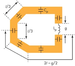
A DGS resonator etched in a metal ground plane is shown in Fig. 1. The open-loop DGS resonator features sharp angles to reduce passive parasitic capacitances and decrease the size of the DGS cell. The open-loop DGS resonator consists of two capacitive arms that are connected via a rectangular metal stub. The etched DGS achieves an equivalent capacitance while the metal area between the two arms achieves an equivalent inductance. The size of the open-loop DGS arm equals 4l – g from Fig. 1. The proposed DGS resonator corresponds to the equivalent-circuit LC model3 demonstrated in Fig. 1.
Values for the resonator’s inductor and capacitor, Lp and Cp, can be computed by means of Eqs. 1 and 27:
Cp = 5fc/π(f20 - f2c) pF (1)
Lp = 250/C(πf0)2 nH (2)
where:
fc = the cutoff frequency (in GHz) and
f0 = the resonant frequency (in GHz) calculated from the transmission characteristics of the quasi-ring DGS slot.
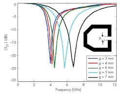
When the quasi-ring DGS slot in the ground plane of Fig. 1 is excited by a 50-Ω transmission line, it performs as a parallel LC resonant circuit10 and also exhibits one-pole bandstop characteristics (Fig. 2). To better understand how changes in the dimensions of the DGC cell affected the behavior of the bandstop filter, a parametric analysis was conducted. For example, Fig. 2 includes the effects of changes in stub width, g, in the open-loop-ring DGS slot on the resonant frequencies of the filter. By changing the width of g, the cutoff frequency and attenuation pole can be readily modified.
The length of the gap (arm) controls the effective capacitance of the microstrip line. As the metal stub width g increases, the cutoff frequency and the attenuation poles shift to higher frequencies. As Fig. 2 shows, the resonant frequency increases from 4.0 to 6.5 GHz as g increases from 3 to 7 mm. As g increases, the effective inductance decreases, so the resonant frequency increases. In this way it can be seen that the stub width g controls the effective inductance, which controls the resonant frequency.
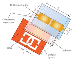
Figure 3 contains a three-dimensional (3D) view of the proposed BSF. The filter consists of two overlapped DGS resonators etched into the bottom layer of the filter circuit, where distance, d, equals 2.5 mm. In addition, two compensating microstrip capacitances on the top layer are connected by means of a 50-Ω microstrip line. Electrical coupling between the two DGS resonators is employed to improve filter performance.
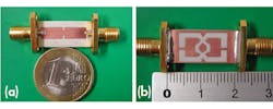
The proposed bandstop filter was fabricated and measured with a model HP8722D vector network analyzer (VNA) from Agilent Technologies (now Keysight Technologies). The filter was printed on Rogers RO4003 PCB material from Rogers Corp. with a relative dielectric constant, εr, of 3.38 measured at 10 GHz through the z-axis (thickness) of the material. The PCB material had a thickness, h, of 0.813 mm. Figure 4 is a photograph of the fabricated BSF.
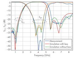
This use of DGS resonators for the BSF makes possible an extremely compact filter. A total area of 0.50λg × 0.25λg is occupied by the filter circuitry, where the wavelength λg equals 38.5 mm. Figure 5 offers a comparison of measured performance with simulations from the commercial simulation software. It is clear from the simulations that the filter’s center frequency equals f0 = 4.1 GHz with a cutoff frequency fc = 2.5 GHz.
The simulated 3-dB stopband bandwidth equals 2.7 GHz. The simulation results showed that the designed filter has good transition characteristics and a symmetrical response (Fig. 5). In addition, the measured stopband return loss and insertion loss are quite respectable: less than -20 dB and 0.7 dB, respectively.
This file type includes high resolution graphics and schematics when applicable.
The results of Fig. 5 show that the use of electric coupling between the two DGS resonators serves to enhance the performance of the BSF, arming it with a wide rejection band and sharp transition from the stopband to the passband. The design strategy produces reflection transmission zeros on both sides of the stopband center frequency to help increase the selectivity of the filter.
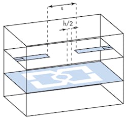
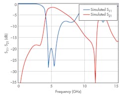
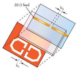
Less-than-positive results were achieved for the BPF; Fig. 6 offers a 3D view of it. The structure has a small gap with distance separation distance, s, equal to 5 mm between the microstrip feeds for which admittance inverter J. In this case, the transmission characteristics are inverted, causing the structure to act as a BPF. Figure 7 offers results of a commercial electromagnetic (EM) simulation program used to analyze this structure. The simulated results show that the filter circuitry behaves much like a bandpass filter, with center frequency f0 at 5 GHz.
The return loss is predicted as being more than 20 dB across the passband from 4.5 to 5.7 GHz, while the simulated passband insertion loss is less than 1.9 dB from 4.5 to 5.5 GHz. Also, there is no spurious passband at 2f0. From the simulation results, two transmission zeros on both sides of the passband can be observed at 3.3 and 11.6 GHz. The BPF simulations show undue losses in the passband and a less-than-ideal upper-transition response. This poor performance can be attributed to poor coupling between the two adjacent DGS resonators.
This file type includes high resolution graphics and schematics when applicable.
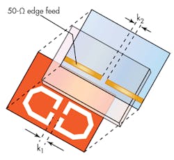
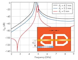
As Fig. 7 shows, the results for the proposed bandpass filter were not very satisfactory. The passband loss is relatively high, while the absence of transmission zeros can be blamed for the lack of passband flatness and transition sharpness. To improve upon these shortcomings, a structure with different topology was designed. An optimized structure was investigated by examining the impact of the external coupling between the feeds and the DGS resonators. This was done by shifting step by step the microstrip feeds from the center of the structure to the edge of the structure, as shown in Figs. 8 and 9.
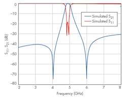
When the feed was moved from the center of the DGS to the edge, the filter characteristics were greatly improved (Fig. 10). Optimum results were achieved when the feed positions were located on the edge of the DGS. By moving the feed positions to the edge of the DGS resonator and using a prober to control the distance, k2, between the two feeds, a BPF with high selectivity can be produced (Fig. 11).
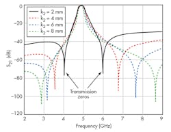
The simulations of this modified filter reveal a center frequency, f0, of 4.9 GHz, with a 3-dB bandwidth of approximately 280 MHz from 4.70 to 5.01 GHz. This filter design also shows low passband insertion loss of around 0.1 dB and excellent response symmetry. The filter design has two transmission zeros at 4 and 6 GHz, located close to the edges of the passband. This provides good selectivity and high stopband rejection for the BPF.
To learn how to adjust the transmission zeros created in the lower and upper stopbands, and thus realize a desired passband bandwidth and to control sharp rejection characteristics, the effects of varying the width of gap k2 on the transmission zeros were studied. Figure 12 shows the dependence of J-inverter width k2 on the positions of the transmission zeros. If all other parameters are kept constant and only k2 is varied, it is relatively easy to control the position of the transmission zeros and the bandwidth and transition sharpness between passband and stopbands.
If k2 increases, the positions of the upper and lower transmission zeros are shifted to higher and lower frequencies, respectively. Similarly, if k2 decreases, the positions of the upper and lower transmission zeros are shifted to lower and higher frequencies, respectively.
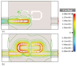
To gain greater insight into the filter design approach with DGS resonators, a near-field distribution of the BPF was computed (Fig. 13). The filter’s electric field was computed for two frequencies, in the passband and stopband regions. At 3.5 GHz, the electric field exhibits high density around port 1 (the input feed port) with no energy flow around port 2, for strong stopband behavior [Fig. 13(a)]. On the other hand, the electric field has high density at 4.8 GHz along the filter structure from ports 1 to 2 (across the DGS resonators) for good passband behavior [Fig. 13(b)]. The electric-field patterns indicate good coupling between the feeds and the DGS resonators.
In summary, the use of DGS resonators made it possible to design and fabricate compact filters in microstrip. A simple transformation from a BSF to a BPF was achieved with the aid of a J-inverter and some external coupling methods applied to the resonators. The computer simulations performed on the filter circuits agree fairly well with measured results, showing that the use of DGS resonators offers great promise for the design of at least two types of compact microstrip filters.
Dr. Ahmed Boutejdar, Associate Professor
Chair of Microwave and Communication Engineering, Otto Von Guericke University of Magdeburg, Magdeburg, Germany
Ahmed A. Ibrahim, Lecturer
Communications and Electronic Engineering Department, Minia University, El-Minia, Eqypt
Dr. Edmund P. Burte, Professor, Chair of Semiconductors and Sensors
Otto Von Guericke University of Magdeburg, Magdeburg, Germany
This file type includes high resolution graphics and schematics when applicable.
References
This file type includes high resolution graphics and schematics when applicable.
1. A. Boutejdar, A. Omar, and E. Burte, “LPF Builds On Quasi-Yagi DGS,” Microwaves & RF, Vol. 52, No. 9, 2013.
2. Lung-Hwa Hsieh, “Tunable microstrip bandpass filters with two transmission zeros,” IEEE Transactions on Microwave Theory & Techniques, Vol. 51 , No. 2, 2003, pp. 520-525.
3. A.A. Elrahman, A.Z. Eldein, A.A. Elmonem, and H. Fathi, “Small size defected ground structure (DGS) coupled resonator band pass filters with capacitor loaded slot using FDTD method,” WSEAS Transactions on Communications, Vol. 10, No. 3, 2011, pp. 88-99.
4. A. Boutejdar, A. Omar, E.P. Burte, R. Mikuta, and A. Batmanov, “DGS and Multilayer Methods Make LPF,” Microwaves & RF, Vol. 50, No. 3, 2011, pp. 61-72.
5. J.-S. Lim, Ch.-S. Kim, Y.-T. Lee, et al. “A new type of low pass filter with defected ground structure,” Technical Program, European Microwave Week, Milan, Italy, September 24-26, 2002.
6. Adel B. Abdel-Rahman, Adel Z. El Dein, Hesham F. A. Hamed, and Ahmed A. Ibrahim, “Small Size Third order coupled resonator band-pass filter using capacitor loaded slots,” IEEE Middle East Conference on Antennas and Propagation (MECAP),Cairo, Egypt, 2010.
7. A. Boutejdar, S. Amari, and A. Omar, “A novel compact J-Admittance inverter coupled microstrip bandpass filter using arrowhead shape as defected ground structure (DGS),” Microwave and Optical Technology Letters, Vol. 52, No. 1, January 2010, pp. 34- 38.
8. Ahmed Boutejdar, “New Method to Transform Band-Pass to Low-Pass Filter Using Multilayer- and U-Slotted Ground Structure (SGS)-Technique,” Microwave and Optical Technology Letters, Vol. 53, No. 10, October 2011, pp. 2427-2433.
9. A.K. Verma and A. Kumar, “Design of low-pass filters using some defected ground structures,” AEU-International Journal of Electronics and Communications, Vol. 65, No. 10, 2011, pp. 864-872.
10. Mouloud Challal, A. Boutejdar, A. Azrar, and Danielle Vanhoenacker-Janvier, “Design of compact low-pass filter with large reject band using open circuit stubs and two-cascaded DGS quasi triangular resonators,” Microwave and Optical Technology Letters, Vol. 55, 2013, pp. 122-127.
11. Dibakar Yadav, Tamasi Moyra, and Kaushik Debbarma, “Microstrip Hairpin Bandpass Filter with Improved Out of Band Performance”, Emerging Trends in Computing and Communication Lecture Notes in Electrical Engineering, Vol. 298, 2014, pp. 27-32.
12. A. Abdel-Rahman, A.K. Verma, A. Boutejdar, and A.S. Omar, “Control of band-stop response of Hi-Lo microstrip low-pass filter using slot in ground plane,” IEEE Transactions on Microwave Theory & Techniques, Vol. 52, March 2004, pp. 1008–1013.
13. A Boutejdar, “Design of broadstop band low pass filter using a novel quasi-Yagi-DGS-resonators and metal box-technique,” Microwave and Optical Technology Letters, Vol. 56, No. 3, 2014, pp. 523-528.
14. A. Boutejdar and A. Omar, “Compensating For DGS Filter Loss,” Microwaves & RF, Vol. 51, No. 2, 2012, pp. 68-76.
15. W.Q. Che, W.J. Feng, and K. Deng, “Microstrip dual-band bandstop filter of defected ground structure and stepped impedance resonators,” International Journal of Electronics, Vol. 97, No. 11, 2010, pp. 1351-1359.
16. Jian-Kang Xiaoa and Yu-Feng Zhub, “Multi-band bandstop filter using inner T-shaped defected microstrip structure (DMS),” AEU International Journal of Electronics and Communications,” Vol. 68, No. 2, February 2014, pp. 90-96.
17. Jia Shen, G. Hong, and M.J. Lancaster, Microstrip Filters for RF/Microwave Applications, second edition, (Wiley, New York, 2004).
18. A. Boutejdar, “New method to transform bandpass to lowpass filter using multilayer-and U-slotted ground structure-technique,” Microwave and Optical Technology Letters, Vol. 53, No. 10, 2011, pp. 2427-2433.
This file type includes high resolution graphics and schematics when applicable.
