Energy-Harvesting Antenna Aids Wireless Sensors
This file type includes high resolution graphics and schematics when applicable.
Energy harvesting is an efficient method for powering different RF/microwave components for communications systems, including antennas. By harvesting energy for such applications as autonomous radio-frequency-identification (RFID) systems and wireless sensors, self-powered solutions can be developed without need of additional batteries. To demonstrate the possibilities, an energy-harvesting patch antenna array was designed to capture as much RF energy as possible from surrounding energy sources.
To minimize costs, the antenna was fabricated on low-cost FR-4 printed-circuit-board (PCB) material. The rectangular patch antenna array was developed for use in the Industrial-Scientific-Medical (ISM) band at 2.45 GHz, employing an additional slot on the rectangular patch element for added gain. The antenna design includes a turn-on light-emitting diode (LED) indicate captured energy at voltages from 0.01 to 3.94 V dc.
Light sensors and other electronic devices using “smart” technologies have already begun to affect many users’ lives. Such sensors detect the level of darkness in a room and automatically turn on the lights at a specific level of light/darkness. This smart system not only helps improve the quality of life, but also contributes to energy and cost savings. This intelligent use of energy can be applied to remote controls without batteries and mobile-telephone chargers that operate with harvested energy.
Researchers have explored various methods for extracting ambient energy from an environment, then converting it into electrical energy for such applications as low-power sensors.1 This scavenging of energy will enable many new “green” electronics devices due to self-powered wireless sensors and autonomous energy.2 Energy is available in the environment for reuse from various sources, including solar power, magnetic energy, vibration, and RF/microwave energy. The latter is freely available in open space; it can be captured by the appropriate receiving antenna and rectified into usable DC voltage.
The use of battery power by a growing number of sensor-based wireless networks and other applications has increased rapidly in recent years, with batteries providing only limited lifespan and fixed energy supply rates. But an energy-capturing antenna, such as a patch antenna, can capture energy from the environment for use in place of the batteries. A number of different patch antennas exist, including meander-line antennas (MLAs),3 linearly polarized antennas,4 and circularly polarized antennas.4 These different configurations will be examined to find the best antenna topology for energy harvesting, along with a circuit capable of converting RF signals into DC voltage for battery replacement.
For maximum coverage, most communications use antennas with omnidirectional radiation patterns. An energy-harvesting system relies on capturing some of this available energy. The amount of available energy is large, but only a small amount can be scavenged due to some energy being dissipated by heat or absorbed by other materials. The RF energy harvesting system consists of a microwave antenna, a prerectification filter, a rectifying circuit, and a DC lowpass filter (LPF) that rectifies incoming electromagnetic (EM) waves into DC current. The rectifying circuit can be any one of several different types—a full-wave bridge rectifier or a single shunt full-wave rectifier, for example.5,6
For optimum power transfer, a LPF is used for impedance matching between the antenna and the rectifier. Once a signal is rectified, a DC LPF is used to smooth the output DC voltage and current by attenuating the high-frequency harmonics present in the RF signals available in the environment. An attempt is made to collect maximum power before delivering it to a rectifying diode; next, the harmonics generated by the diode, which radiate from the antenna as lost power, are suppressed.6
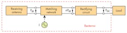
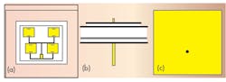
A number of factors impact effective energy harvesting, including antenna transmitted power, antenna received power, conversion efficiency, and conversion circuit analysis.7 To increase the conversion efficiency, several antenna designs must be implemented, including antenna arrays and circularly polarized antennas. The broadband antenna receives relatively high RF power from various sources, while the antenna array increases the incident power delivered to the diode for rectification.6,7Figure 1 shows a block diagram of the rectenna.
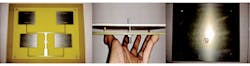
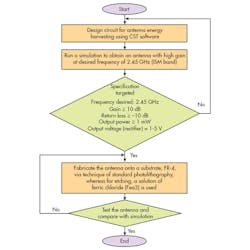
The CST Microwave Studio Suite 2011 from Computer Simulation Technology was used for designing and simulating the high-gain energy-harvesting antenna, while the Advanced Design System (ADS) 2011 software from Keysight Technologies was used for design and simulation of the rectifying circuit. The antenna and rectifying circuits were fabricated on FR-4 PCB material for comparison of actual measurements with simulations. Figure 2 shows the flow of the antenna design process.
This file type includes high resolution graphics and schematics when applicable.
Designing the Antenna
This file type includes high resolution graphics and schematics when applicable.
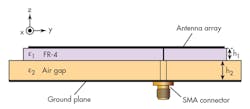
The antenna was designed for ISM-band applications and was fabricated on the low-cost circuit substrate material using photolithography patterning and etching techniques. As Fig. 3 shows, the antenna consists of a bottom ground plane, an air gap between the FR-4 circuit substrate and the microstrip patch, and an additional slot. The patch and the ground plane are comprised of copper. The antenna is excited by a coaxial feed connector at the center of the transmission line. For use at 2.45 GHz, the width and the length of the microstrip patch have been calculated by the following formula (given in ref. 9):
W = c/{2f0[(εr+ 1)/2]0.5}
Leff = c/[2f0(εr eff)0.5]
where
c = the speed of light;
f = the operating frequency (2.45 GHz);
εr = the relative dielectric constant of the PCB substrate; and
εr eff = the effective relative dielectric constant of the PCB substrate.
For good isolation, the antenna’s adjacent elements should be separated by at least one-half wavelength (λ/2) at the desired frequency. Isolation tests were performed for antenna-element spacing of 5.8 cm (0.4737λ), 6.1 cm (0.4982λ), and 6.5 cm (0.5310λ). A spacing, x, of 6.1 cm was found to provide the best performance after optimization.
Microstrip antennas are often employed not only as single-element components, but also as arrays—especially when needed to create a pattern that cannot be achieved with a single-element antenna. The feed network for the microstrip array can be accomplished by using tapered lines to match 100-Ω antenna patch elements to a 50-Ω input port or to quarter-wavelength impedance transformations.
The current design employs tapered lines with the antenna array fed by a probe in the middle of the thickest transmission line, at an SMA-compatible impedance of 50 Ω. The dimension of the transmission line was calculated using the formula from ref. 10. For a characteristic impedance of Z0 = 50 Ω, the impedance that is split into both feed lines is 100 Ω.
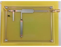
The design of the rectifying circuit was based on transmission-line calculations for the circuit. The basic rectifier design for the energy-harvesting system consists of one diode and one capacitor. This simple design was chosen to minimize diode losses. A model HSMS-286B diode from Agilent Technologies (now Keysight Technologies) was selected for its fast switching speed and low voltage drop.
Sampling Simulations
A parametric study approach was applied to ensure that the antenna operated at the required resonant frequency (2.45 GHz). Using this design method, adjustments were made to the length and width of the patch, as well as to the slot and length of the transmission line. The effects on return loss, gain, and impedance bandwidth were noted. The initial design was without the additional slot and the antenna operated at 2.4973 GHz with return loss of -12.178 dB. The fractional bandwidth was calculated as 2.96%, and antenna gain was 13.35 dB.
An additional slot was introduced to each single element of the antenna array to improve performance, per ref. 11; by doing so, the additional slot improved the antenna gain to 13.51 dB. Parametric analysis was performed with fixed design parameters, except for length and width parameters Lf, Lb, Lp, Wp, and Ls1.
The following values were applied to the antenna design: Lp = 45 mm, Lf = 25.5 mm, and Wp = 49 mm. The design was then simulated and the return loss was found to improve to -46.486 dB at 2.408 GHz. The calculated impedance bandwidth was 3.65% and the gain was 13.54 dB with 14.04-dB directivity.
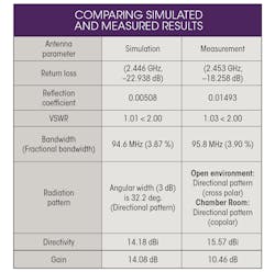
The antenna performance was then simulated using values from the parametric studies, and high gain was found for the antenna design with an additional slot and with values of Wp = 47 mm, Lp = 43 mm, Lf = 25.5 mm, and Ls1 = 16 mm. This antenna operates at 2.446 GHz with -22.938 dB return loss and 99.4-MHz (3.87%) impedance bandwidth. It yielded high gain of 14.08 dB with 14.18-dB directivity.
When only Lp was changed (to a value of 41 mm), the gain dropped to 13.79 dB. Some frequency shifting was observed: to 2.486 GHz with return loss of -15.931 dB. This indicated that the length of the patch affected frequency. Thus, to ensure operation in the ISM band at 2.45 GHz, Lp was set at 43 mm. The impedance matching for the antenna design at 2.446 GHz was 59.499326 – 8.460473 Ω with a line impedance, S1, of 61.18 Ω.
This file type includes high resolution graphics and schematics when applicable.
Making Measurements
This file type includes high resolution graphics and schematics when applicable.
The antenna and rectifying circuit were measured separately before being integrated and measured again. Figures 5 and 6 show the measurements of the output voltages of the rectifying circuit before and after this integration. Measurements were performed to determine return loss, radiation pattern, gain, and received power for the antenna array.
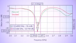
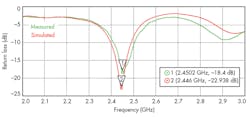
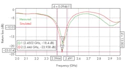
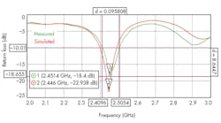
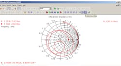
The antenna array was designed to operate with single-band functionality at 2.45 GHz for ISM-band applications.12,17Figure 7 shows simulation and measurement results where the x-axis is frequency (GHz) and y-axis is return-loss magnitude (dB). Simulation indicated the best operating frequency as 2.446 GHz with -22.938 dB return loss. Measurements indicated that the antenna resonates best at 2.4502 GHz with -18.4 dB return loss. The measurements appeared to show 95% accuracy and nearly the same values as the simulation results. The optimum return loss was achieved with the introduction of the slot from ref. 18 and the corporate-feed-network method detailed in ref. 19.

The antenna bandwidth was determined at the upper frequency minus the lower frequency, both at their 3-dB-down points, as shown by simulation and measurement. Figures 8 and 9 reveal the simulated and measured antenna bandwidths as 94.6 and 95.8 MHz, respectively. The measured results are slightly better than the simulation results, but both values are still relative similar. The bandwidth could be increased further by the use of a double slot introduced for each of the radiating elements in the patch antenna array and feed location in the feed network arrangement.20
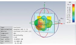
The desired gain for this multilayer 2 × 2 antenna array, with additional slot for each of the radiating elements, was greater than 10 dB, for good results when harvesting ambient RF energy. Theoretically, antenna gain depends on total power delivered to an antenna input terminal. Thus, by simulation (Fig. 10), antenna gain of 14.08 dB was realized for a three-dimensional (3D) far-field view. The simulation of Fig. 11 shows that the antenna yields high directivity of 14.18 dBi.
The directivity of each receiving antenna element is important where each must be directed, so that its maximum gain lobe is pointed towards the transmitting antenna to optimize the amount of received energy. An arbitrary minimum gain of 3 dB, which is the half-power beam width (HPBW), was chosen for the receiving antenna of the energy harvesting system.21 Improvements in gain and directivity were due to the multilayer circuit structure used in the design, in which an air gap is placed between the FR-4 substrate and multislotted microstrip patch antenna.22
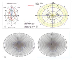
The antenna’s radiation patterns also were simulated and measured. Based on the simulations of Fig. 12(a), the antenna radiates/receives RF energy in a directional pattern which radiates more efficiently in some directions than in others. The HPBW (at 3 dB) is 32 deg. (see table); such a narrow beam width is the result of the thin FR-4 substrate material used for the antenna. The magnitude of the antenna’s main lobe is important, and the side lobe level must be reduced since it comes from an undesired direction.
Figures 12(b) and (c) compare measurements of the antenna in the open environment and in a test chamber. In both cases, the current in the antenna shows that the main radiating elements are at inside edges and near the probe feed.23 As a result, the antenna offers a more directional radiating pattern and must be placed precisely near a transmitting antenna.
Impedance matching and even flow of surface currents are important for this antenna. Theoretically, an EM wave that travels through different parts of the antenna system may encounter differences in impedance. The matching process is necessary to transform the antenna’s input impedance to the same impedance value for its transmission lines. Therefore, the antenna must be integrated with the rectifying circuit in terms of impedance. Without good impedance matching, some wave energy will be reflected and the rectifying circuit will not have the energy available to convert to DC voltage.
This ISM-band energy harvesting antenna showed good agreement between simulated and measured results. The antenna system, which consists of an antenna and rectifying circuit, operates at 2.4514 GHz with measured output voltage of 3.94 V dc. It is a design that shows good potential for use in a variety of ISM-band applications that could possibly be freed of their needs for batteries.
M.S. Jawad, Doctor, Senior Lecturer
Nurzaimah Binti Zainol, Research Assistant
Z. Zakaria, Associate Professor
Department of Telecommunication, Faculty of Electronic and Computer Engineering, University of Technical Malaysia Melaka, Karung Berkunci 1200, 75450 Ayer Keroh, Melaka, Malaysia
This file type includes high resolution graphics and schematics when applicable.
References
This file type includes high resolution graphics and schematics when applicable.
1. N.M. Din, C.K. Chakrabarty, A. Bin Ismail, K.K.A. Devi, and W.-Y. Chen, “Design of RF Energy Harvesting System for Energizing Low Power Devices,” Progress In Electromagnetics Research, Vol. 132, 2012, pp. 49-69.
2. Z. Zakaria, N.A. Zainuddin, M.Z.A. Abd Aziz, M.N. Husain, and M.A.Mutalib, “Dual Band Monople Antenna For Energy Harvesting System,” IEEE Papers, Centre of Telecommunication Research and Innovation (CeTRI).
3. D. Misman, M.Z.A. Abd Aziz, M.N. Husain, and P.J. Soh, “Design of Planar Meander Line Antenna,” 3rd European Conference on Antennas and Propagation (EuCAP), Berlin, Germany, 2009, pp. 2420-2424.
4. M.Z.A. Aziz, N.A D.A. Mufit, M.K. Suadi, A. Salleh, and M.K.A. Rahim, “Study on Microstrip X-Linear Polarized and X-Circular Polarized Antenna,” Sixth European Conference on Antennas and Propagation (EuCAP 2012), Prague, Czech Republic, 2012, pp. 907-911.
5. M. Arrawatia, M. S. Baghini, and G. Kumar, “RF Energy Harvesting System from Cell Towers in 900 MHz Band,” 2014 IEEE International Conference on RFID (full paper not yet available).
6. S. Shrestha, S. K. Noh, and D. Y. Choi, “Review Article: Comparative Study of Antenna Designs for RF Energy Harvesting,” International Journal of Antennas and Propagation, 2013, Article ID 385260, Hindawi Publishing Corp., 10 pp.
7. R. Dahiya, A.K. Arora, and V.R. Singh, “RF Energy Harvesting for Hybrid Application: Review and Analysis,” May 3013. International Journal of Innovative Technology and Exploring Engineering (IJITEE), Vol. 2, No. 6, ISSN: 2278-3075.
8. Dau-Chyrh Chang, Bing-HaoZeng, and Ji-Chyun Liu, “High Performance Antenna Array with Patch Antenna Elements,” PIERS Proceedings, March 22-26, 2010.
9. Chandan Kumar Ghosh, Susanta Kumar Parui, “
10. David M. Pozar, Microwave Engineering, 4th ed.,(Wiley, New York, 2014), pp. 143-148.
11. Chandan Kumar Ghosh and Susanta Kumar Parui, “
12. Standard Radio System Plan, “MHz to 2400 MHz,” Malaysian Communications and Multimedia Commission, SKMM SRSP-532 BWA, Rev. 1, October 15, 2009, p. 10.
13. Hu-Cheng Sun, Yong-XinGuo, and Zheng Zhong, “A High-Sensitivity 2.45 GHz Rectenna for Low Input Power Energy Harvesting,” IEEE Antennas and Wireless Propagation Letters, Vol. 11, 2012.
14. Gianfranco Andia Vera and Apostolos Georgiadis, “Design of a 2.45 GHz Rectenna for Electromagnetic (EM) Energy Scavenging,” 2010 IEEE Antennas and Wireless Propagation Letters, Vol. 9, 2010, pp. 444-446.
15. Hu-Cheng Sun, Yong-XinGuo, and Zheng Zhong, “A High-Sensitivity 2.45 GHz Rectenna for Low Input Power Energy Harvesting,” IEEE Antennas and Wireless Propagation Letters, Vol. 11, 2012.
16. Md. Abu Baker and Siddique Akhanda, “Design of a High Gain Microstrip Patch Antenna for WLAN/Bluetooth Applications at 2450 MHz Frequency,” International Journal of Scientific & Engineering Research, Vol. 4, No. 8, June 2013.
17. Ahmed Al-Shaheen, “New Patch Antenna for ISM Band at 2.45 GHz,” ARPN Journal of Engineering and Applied Sciences, Vol. 7, No. 1, January 2012.
18. J.I. Moon and I.K. Cho, “Design of efficient rectenna with vertical ground-walls for RF energy harvesting,” Electronics Letters, Vol. 49, No. 17, August 15, 2013.
19. Fangyi Xie Optimal, “Design of an Antenna Array for Energy Harvesting,” IEEE Antennas and Wireless Propagation Letters, Vol. 12, 2013.
20. Liang Zhu, Yong Cheng, “A Novel High-Gain Wideband Patch Antenna Fed by Twin-L-probe,” IEEE International Conference on Microwave and Millimeter-Wave Technology (ICMMT), 2010.
21. Zhi Wei Sim, “Investigation of PCB Microstrip Patch Receiving Antenna for Outdoor RF Energy Harvesting in Wireless Sensor Networks,” IEEE Antennas & Propagation Conference, Loughborough, England, 2009.
22. Xiaoang Li and Chao Li, “Design of High Gain Multiple U-Slot Microstrip Patch Antennas for Wireless System,” Proceedings of 2010 International Conference on Computational Problem Solving, December 2010, Lijiang, China.
23. NeÅem Keskin, “E-Shaped High Gain Microstrip Patch Antenna,” Proceedings of the 2012 Applied Computational Electromagnetics Society (ACES) conference.
This file type includes high resolution graphics and schematics when applicable.
