Millimeter-Wave Technology Prepares For A Wealth Of Applications
This file type includes high resolution graphics and schematics when applicable.
Millimeter-wave technologies will soon touch virtually every industry. Until recently, the semiconductor and machining capabilities of manufacturers were too inaccurate or cost prohibitive to enable millimeter-wave device production for all but specialized applications. Now, advances in semiconductor technology, testing techniques, and micromachining are beginning to bring millimeter-wave solutions to a wide range of applications. The growth of the global millimeter-wave technology market in terms of revenue is expected to reach $1.1 billion in 2018 at a CAGR of 59.10%. Millimeter-wave product volumes are estimated to grow from roughly 11,800 units to more than 360,000 units in 2018. Alongside this growth, the demand for high-data-rate technologies for wireless backhaul is driving innovation in the unlicensed 57-to-64-GHz frequency band.
Related Articles
• Air and Missile Defense Radar Market to Reach $10.4 Billion By 2020
• Dual-Layer Materials Suppress EMI Noise
• 3D Micromachined Subsystems Enable mm-Wave Components
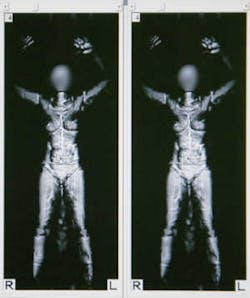
For decades, millimeter-wave technology has been implemented in many military, aerospace, meteorology, and satellite applications. Mono-pulsed radar systems and weather radiometers were very common. Another example of applied millimeter-wave technology is the imaging of objects in space with large radar installations that pick up millimeter-wave radiation. Discrete satellite-to-satellite communications also is enabled by highly directional millimeter-wave signals. More recently, homeland security has been using millimeter-wave imagers for security screeners (Fig. 1). Because millimeter-wave energy is non-ionizing and depletes rapidly in the environment (thanks to the molecular absorption of atmospheric oxygen), the technology can be safely used to image metallic and non-metallic objects on people.
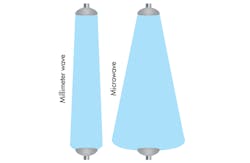
The rapid atmospheric attenuation of millimeter-wave signals also can benefit high-speed wireless-technology links by limiting interference between transceivers. The dimensions of millimeter waves lead to very directional and high-gain antennas. Such antennas, in turn, translate into lower levels of interference and higher data rates (Fig. 2). These millimeter-wave properties have nurtured the development of a variety of short- to mid-range high-speed data-link technologies (Fig. 3). Development is being focused on applications for these high-speed data links, such as pico-cell wireless, wireless backhaul, chip-to-chip communication, and higher-performing RF electronics.
The increased interest in these data links also has been driven by the limited licensing issues in the unlicensed 60-GHz band as well as the lightly licensed frequencies from 71 to 76 GHz and 81 to 86 GHz. These frequency bands require a very minimal cost per license or no license at all, depending upon where the links are in the world. There are, however, constraints in transmit power in accordance with the Maximum Permissible Exposure (MPE) limits. Technical complexities also arise when maintaining a stable output power level at millimeter-wave frequencies.
Because these technologies have a wealth of bandwidth options in which to operate their links, fully duplex data rates beyond the common 1.25 Gbps are possible. Less spectral clutter also enables the use of modulation schemes, such as direct digital modulation, which lead to lower communication-electronics costs. This is detailed in the Shannon-Hartley theorem in the equation:
C = B log (1 + S/N)
where C is the channel capacity in bits per seconds, B is the bandwidth in hertz, S is the average received signal power over the bandwidth in watts, and N is the average noise figure over the bandwidth in watts.
It is evident in the equation that even with lower signal power, the lack of interference noise and the ability to use a very wide bandwidth can offer a very-high-capacity channel link. The atmospheric absorption does limit these devices to a range of a few hundred to a few thousand meters when used in a directional manner. The very narrow transmission beam also requires that the alignment between the two transceivers is accurate. For this reason, companies like HXI provide gun-sight mounts on their HDTV-link systems. These links have an aggregate throughput of 2.97 Gbps with a two-channel unit and an operating range from 20 to 300 m. For omnidirectional scenarios, like wireless Internet, the range is limited to tens of meters.
In the telecommunications arena, more carriers are employing Long-Term-Evolution (LTE) networks to meet the data demand for mobile broadband. Small-cell solutions also are increasingly being adopted to service the higher-demand areas that are not being fully served by larger macrocells. Offering these services in congested areas—either in-building or externally—is often prohibitively expensive to implement with fiber-optic cabling. And it is impossible to service the growing capacity demands with slower-speed passive cabling. Using fiber-optic-speed millimeter-wave solutions is a proposed method for offering wireless backhaul in these difficult-to-service areas with minimal cost compared to other solutions. The available bandwidth also may eventually allow data rates as high as 40 Gbps.
This file type includes high resolution graphics and schematics when applicable.
Benefits Of Size Savings
This file type includes high resolution graphics and schematics when applicable.
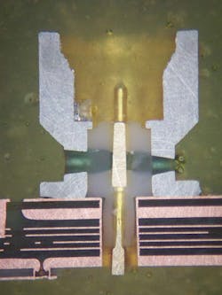
Another advantage of millimeter-wave devices is the relative size of the antennas and the device components. These compact components can be very light and portable, which opens doors to more environments in which millimeter-wave devices could be used. On the other hand, the wavelength dimensions of these signals require very precise tolerances on small components (Fig. 4). According to Mark Faulkner, Microsemi’s vice president of RF integrated solutions engineering, “There are tiny features in a waveguide end launch. I have designed and built these things up to Q band. The elements and machined parts look like a grain of pepper, they are so tiny. Imagine gold plating that and screwing it down or attaching it somehow. It is a challenge.”

The skin effect causes these higher-frequency waves to travel at the surface of the conductors, making surface finish and plating serious concerns. Small imprecisions in machining also lead to very low yields and higher costs. A solution to these problems has been to develop semiconductor-based millimeter-wave systems and other micro-fabrication techniques.
Another growing trend has been to implement on-chip antennas with self-testing electronics to cut down on expensive millimeter-wave test. Companies like IBM and United Monolithic Semiconductors have implemented processes with tool support for enabling millimeter-wave design as well as digital integration. Testing systems like digital-signal processing, internal noise sources, and loop-back sensing methods can all enable a self-testing device. IBM’s 9HP process uses silicon-germanium (SiGe) BiCMOS for this integration. Other semiconductors used for millimeter-wave electronics are implemented in gallium arsenide (GaAs), indium phosphide (InP), and gallium nitride (GaN).
Related Articles
• Air and Missile Defense Radar Market to Reach $10.4 Billion By 2020
• Dual-Layer Materials Suppress EMI Noise
• 3D Micromachined Subsystems Enable mm-Wave Components
When working with semiconductor components, difficulties often arise when interfacing to the external electronics or antenna. To manage some of these challenges, companies like Nuvotronics have developed highly refined micro-fabrication methods to create complete millimeter-wave structures in a monolithic process. Nuvotronics claims that its PolyStrata manufacturing technology can be used to make 3D transmission lines with advanced routing while enabling other features with 3D stacking. In addition to being able to create an effective millimeter-wave interface, millimeter-wave surface-mount-technology (SMT) components and other monolithic microwave integrated circuits (MMICs) can be included in the 3D design.
With these advanced fabrication techniques, millimeter-wave devices could soon be found in many commercial and industry environments. With the potential for integrated, ultra-high-speed data connections and low transmission power, this technology also could enable the Internet of Things and Big Data revolutions. At this point, the major factor limiting the adoption of millimeter-wave systems is the cost. “That is one of the fun challenges for me,” Faulkner says, “getting the cost out of these components. If you get the costs low enough, you can enable a market and open up a larger use for these devices.”
Millimeter Waves Enhance Security
Other benefits of millimeter-wave technology include extremely low energy levels of radiation and the ability to generate high-resolution images. These stand-off imagers can also be implemented as passive radiometers, as our bodies naturally radiate millimeter waves. “Passive radiometers take advantage of thermal radiation,” Faulkner explains. “They are completely harmless. Just by the virtue of you having temperature, you are emitting radiation. These passive sensors can take advantage of that.” These devices can be packaged in a small and energy-efficient package deployable in a handheld scanner, such as Microsemi’s Allclear Handheld scanner. Such imagers can be employed in security screening scenarios that quickly and safely inspect individuals and their possessions. Unlike many other security screening technologies, millimeter-wave imagers can be designed into portable platforms and used as standoff imagers.
This file type includes high resolution graphics and schematics when applicable.
About the Author
Jean-Jacques DeLisle
Jean-Jacques graduated from the Rochester Institute of Technology, where he completed his Master of Science in Electrical Engineering. In his studies, Jean-Jacques focused on Control Systems Design, Mixed-Signal IC Design, and RF Design. His research focus was in smart-sensor platform design for RF connector applications for the telecommunications industry. During his research, Jean-Jacques developed a passion for the field of RF/microwaves and expanded his knowledge by doing R&D for the telecommunications industry.
