Combining and dividing signal power has long been an important function in electronic systems ranging from commercial communications networks to space-based systems—essentially, wherever signals must be summed or distributed. Power dividers and combiners can be as simple as compact two-way components that split an input signal into two equal output signals each at one-half the power level of the input signal. They also can be quite complex, as evidenced by the multiway power combiners and dividers used in such applications as commercial in-building wireless communications networks and military phased-array radar systems.
By meeting some of the more complex requirements by squeezing power combiner/divider performance into compact housings, Renaissance Electronics & Communications (REC) is able to supply RF/microwave power dividers/combiners that meet a wide range of needs, while also saving space in target applications.
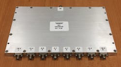
As an example, model 10A3NB-8S is an eight-way power divider (see figure) with tapered output levels, as might be used for phased-array applications. Designed for L-band use from 1100 to 1500 MHz in radar and communications systems, it works without attenuators, but divides input signals into outputs that are reduced by 18.4 dB, 12.4 dB, 8.6 dB, 6.7 dB, 6.7 dB, 8.6 dB, 12.4 dB, and 18.4 dB across the eight output ports.
Isolation between ports is 18 dB, and the eight-way divider exhibits VSWR of 1.43:1. It is designed to feed a fixed antenna with those eight staggered output signal levels. The unit handles 35 W CW input power and 350 W peak input power, and saves space by packing eight channels of power division into a housing measuring just 8.0 × 5.0 × 0.5 in.
Signals often must be processed across a range of frequency bands, so having a single power combiner that can handle multiple frequency bands can save the spaces for several components within the system. One example of this design approach is the model 16A4NAR multiple-band power combiner, designed for low passive-intermodulation (PIM) performance. It is actually the equivalent of three separate power combiners, since it covers frequency bands of 806 to 960 MHz, 1,710 to 1,880 MHz, and 1,920 to 2,170 MHz with low loss and high isolation. The maximum insertion loss is 0.2 dB through 960 MHz and 0.5 dB from 1,710 through 2,170 MHz.
This wireless communications systems combiner handles power levels to 240 W average power. The frequency bands are well isolated from each other, with 65-dB separation from the band at 806 to 960 MHz and the bands at 1,710 to 1,880 MHz and 1,920 to 2,170 MHz. The band from 1710 to 1880 MHz is separated by 70 dB from the band at 806 to 960 MHz and by 65 dB from the band at 1,920 to 2,170 MHz. The band from 1,920 to 2,170 MHz is isolated by 70 dB from the 806-to-960-MHz band and by 65 dB from the 1,710-to-1,880-MHz band. The power combiner has typical PIM performance of -160 dBc when tested with two tones at 20 W each.
Although somewhat larger than the eight-way power divider, at 300.0 × 168.0 × 59.0 mm, this combiner can save space in a system by processing signals from multiple communications bands. It is designed for operating temperatures from -30 to +65°C and weighs 2.5 kg.
When space is tight, the firm offers multiple functions within a single housing. One such example is the model 10A4BV integrated switch and power divider, which operates from 380 to 2850 MHz with 120-dB isolation from the input to the output port. It is ideal for modulated signal testing on radios or amplifiers, combining and switching two ports while maintaining high isolation.
It is rated for input power levels to about 2 W (+33 dBm) on each port, with a damage level of about +34 dBm on each. The combination component has less than 2.5 dB insertion loss across its frequency range; the switch is controlled by means of +3.3-VDC transistor-transistor-logic (TTL) signals. The unit, which measures 4.00 × 4.00 × 1.13 in., operates on 0.6 mA current at +3.3 VDC.
Renaissance Electronics & Communications, LLC, 12 Lancaster County Rd., Harvard, MA 01451; (978) 772-7774, FAX: (978) 772-7775
