Single CDTA Leads To Multiple Filters
This file type includes high resolution graphics and schematics.
Electronically tuned filters can be implemented with a versatile circuit known as a current differencing transconductance amplifier (CDTA). In fact, it is possible to realize a filter design that is capable of providing all of the standard filter functions—including lowpass, highpass, bandpass, bandstop, and all pass functions—from the same CDTA without the need of component matching conditions, nor having to change circuit topology. The natural frequency of the filter can be tuned electronically by varying the bias current to the CDTA.
Filters of many different response types are widely used in high-frequency circuits. For that reason, having a circuit that can double as several different types of filters can be quite useful for a variety of applications (in commercial, industrial, and even military circuits). Based on an active component, a CDTA, the natural frequency (ω0) of this filter design is modified simply by changing the bias current to the amplifier.
Related Articles
• Single Filter Has Many Responses
• Ensure Success In SAW-Filter Choices
• Compact Switched Filters Hit 8 GHz
Introduced more than a decade ago, CDTAs are active building blocks with two current inputs and two kinds of current outputs.1 They have been used in various designs since their introduction, with many active biquad circuits implemented by means of CDTA.2-8 In fact, the literature has reported on the use of a small number of active and passive components as part of a KHN filter,2,3—although its highpass responses were not at high output impedances, and the design approach did not support bandstop and allpass filter responses. A multiple-input, single-output filter was unveiled in the literature,4-6 capable of realizing all of the biquad filter responses simultaneously, although it required a large number of active components. A multifunction filter with a minimum number of devices was proposed in the technical literature,7 but it required some modifications to the topology to implement the different filter responses. Even though work previously performed with only one CDTA achieved all of the different filter responses, it required a large number of passive components.8
One goal of this current report is to provide those different filter responses, with reduced power consumption and manufacturing cost, using a multiple-input, single-output multifunction biquad. The filter construction employs a single CDTA as the active component, along with two resistors and two capacitors as the passive circuit elements. The proposed configuration can implement all the filter responses simultaneously (i.e., lowpass, highpass, bandpass, and bandstop responses).The nature frequency (ω0) can be electronically adjusted tunable transconductance. The circuit enjoys low active and passive sensitivities.
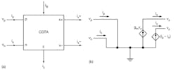
1. These diagrams show the symbolic representation of the CDTA (a) along with its equivalent circuit (b).
Figure 1 shows the circuit representation and equivalent circuit of the CDTA. The terminal expression can be defined by the equalities in Eq. 1:

The input terminals are represented by p and n, while the output terminals are identified by z and x. Parameter gm represents the transconductance gain of the CDTA, while vz = iz × zz with zz represents the external impedance connected to terminal z. The differential current, ip - in, is applied to the input terminals and flows over to terminal z where an external impedance is connected to this node. The voltage drop at terminal z is transferred to a current at terminal x, ix, by means of a transconductance parameter, gm; the latter is electronically controlled by an external bias current, IB.
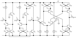
2. This schematic diagram shows the bipolar circuit of the CDTA.
Figure 2 shows the possible bipolar realization of the CDTA detailed in this work. The circuit consists of a current-differencing circuit, Q1 - Q11 and a transconductance amplifier, Q12 - Q33. In this case, the transconductance gain, gm, is directly proportional to the external bias current, IB, which can be written as Eq. 2:

where VT = 26 mV at +26°C is the thermal voltage.
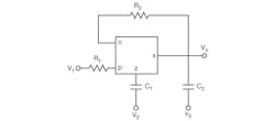
3. This is the simple schematic diagram for the CDTA-based three-input, single-output multifunction filter.
Figure 3 shows the proposed CDTA-based three-input, single-output multifunction filter. The topology is very simple; all the second-order filter responses can be realized simultaneously without changing circuit components. Equation 3 offers the mathematical basis for the different filter responses based on the transconductance gain:

Referring to Eq. 3, a lowpass function is obtained when V1 = Vin and V2 = V3 = 0. The bandpass response is obtained when V2 = Vin and V1 = V3 = 0. The highpass function is possible when V3 = Vin and V1 = V2 = 0. The bandstop function is achieved when V1 = V3 = Vin and V2 = 0. The allpass filter function is obtained when V3 = V1 = -V2 = Vin. The natural angular frequency and quality factor of the filter can be found from Eq. 4:

From Equation (4), it is possible to find that the different filter responses can be electronically tuned by altering the amplifier’s transconductance gain through bias current IB. By taking into account the non-idealities of the CDTA in terms of frequency, the port relations in Eq. (1) can be rewritten as Eq. 5:

where:
ap = 1 - εp and
εp(|ε| × 1) denotes the current tracking error from p to z and
an = 1 - εn and
εn(|εn| × 1) denotes the current tracking error from n to z of the CDTA, respectively. Reanalyzing the filter presented in Fig. 3, the denominator polynomials of the transfer functions can be described as shown in Eq. 6:

In this case, the modified parameters ω0 and ω0/Q are rewritten as Eq. 7:

Meanwhile, the active and passive sensitivity of the presented configurations are:

From the above sensitivity figures, it turns out that the circuit enjoys very low active and passive sensitivities.
To testify the theoretical analysis, the proposed circuits have been simulated by PSPICE program. The CDTA were performed by the schematic bipolar implementation given in Fig. 2 with the transistor model parameters of PR100N (PNP) and NP100N (NPN) of the bipolar arrays ALA400 from AT&T.9 The supply voltages are ±V, and the bias currents re IA = IC = 100 μA.
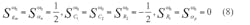
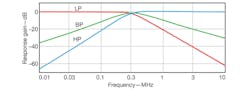
To ease simulation, the capacitance was set so that C1 = C2 = 1 nF while R1 was set at 1 kΩ, R2 = 0.5 kΩ, and the transconductance gain value was set at gm = 2 mA/V(IB = 100 μA). Figure 4 shows the simulated frequency responses of the lowpass, bandpass, and highpass filter configurations, while Fig. 5 shows the bandstop filter response for the proposed filter.
4. These are simulated current responses for CDTA-based filter’s lowpass, bandpass, and highpass responses.
5. These are simulated current responses for CDTA-based filter’s bandstop responses.
In summary, this biquad filter construction can serve as a number of different filter types, electronically tuning the responses by adjusting the external bias current to the filter’s active component, a CDTA. The filter’s performance was simulated with the aid of PSPICE simulation software from Cadence Design Systems which reinforces the performance expected from theory. The CDTA-based filter circuit offers very low active and passive sensitivities, and no component matching is required.
Xin Liu, Masters Degree Candidate
College of Information Science and Engineering, Hunan University, Changsha, Hunan, People’s Republic of China; e-mail: [email protected]; +86 134 6765 6813.
Heizen He, Professor
College of Information Science and Engineering, Hunan University, Changsha, Hunan, People’s Republic of China.
Chunhua Wang, Professor and Doctoral Supervisor
College of Information Science and Engineering, Hunan University, Changsha, Hunan, People’s Republic of China.
Acknowledgment
This work is supported by the National Natural Science Foundation of China (No. 61274020).
References
1. D. Biolek, “CDTA—building block for current-mode analog signal processing,” Proceedings of the ECCTD’03 , Krakow, Poland, Vol. III, 2003, pp. 397–400.
2. A.U. Keskin, D. Biolek, E. Hancioglu, and V. Biolkova, “Current-mode KHN filter employing current differencing transconductance amplifiers,” International Journal of Electronic Communications (AEU), Vol. 60, 2006, pp. 443-446.
3. D. Biolek, V. Biolkova, and K. Kolka, “Current-mode biquad employing single CDTA,” Indian Journal of Pure and Applied Physics, Vol. 47, 2009, pp. 535-537.
4. N.A. Shah, M. Quadri, and S.Z. Iqbal, “CDTA based universal transadmittance filter,” Analog Integrated Circuits and Signal Processing Journal, 2007, pp. 65-69.
5. W. Tangsrirat, T. Dumawipata, and W. Surakampontorn, “Multiple-input single-output current-mode multifunction filter using current differencing transconductance amplifiers,” International Journal of Electronic Communications (AEU), Vol. 61, 2007, pp. 209-214.
6. W. Tanjaroen, T. Dumawipata, and W. Tangsrirat, “TISO cascadable current-mode multifunction filter employing current differencing transconductance amplifiers,” in Proceedings of SICE-ICASE International Joint Conference. Bexco (Korea), 2006, pp. 5703-5706.
7. N.A. Shah, M. Quadri, and S.Z. Iqbal, “Current-mode multifunction filter using current differencing transconductance amplifier,” Indian Journal of Pure & Applied Physics, Vol. 45, No. 9, September 2007, pp. 767-769.
8. D. Prasad, D.R. Bhaskar, and A.K. Singh, “Multi-function biquad using single current differencing transconductance amplifier,” Analog Integrated Circuit Signal Processing, available online, DOI 10.1007/s10470-009-9310-1.
9. D.R. Frey, “Log-domain filtering: an approach to current-mode filtering,” IEEE Proceedings G: Circuits, Devices, and Systems, Vol. 140, 1993, pp.406-416.
This file type includes high resolution graphics and schematics.
