Split-Ring Resonators Add to SIW Bandpass Filter
This file type includes high resolution graphics and schematics when applicable.
Waveguide has long been a reliable, low-loss transmission line technology capable of handling high power levels and forming high-quality-factor (high-Q) resonators. But it is large and heavy compared to transmission-line technologies constructed on printed-circuit-board (PCB) materials. Substrate-integrated-waveguide (SIW) transmission-line technology brings some of the features of rectangular waveguide to the miniature size of PCB circuits.
In addition, SIW transmission lines are easy to fabricate. By using SIW transmission lines to fabricate complementary split-ring resonator (CSRR) structures, it is possible to achieve waveguide-like filter performance from a planar PCB.

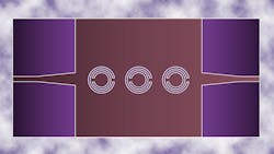
As with metallic waveguides, SIW circuits with CSRR elements are capable of achieving high-quality-factor (high-Q) performance. By combining SIW technology with CSRR circuit elements, it is possible to build a low-profile planar bandpass filter on a single substrate with high-Q performance for radio front ends in broadband communication systems (Fig. 1).
CSRRs etched in the ground plane or conductor strip of a planar transmission media, such as microstrip or coplanar waveguide (CPW), provide a negative effective permittivity to the structure. In doing so, they preclude signal propagation and provide stopband behavior at the resonant frequency of the CSRR structure.1
CSRRs have been proposed for the synthesis of negative permittivity and left-handed (LH) metamaterials in planar configurations.1-3 CSRRs are the dual counterparts2 of the split-ring resonators (SRRs) proposed by Pendry in 1999.4 CSSRs have been applied to the design of compact bandpass filters with high performance and controllable characteristics.5-6
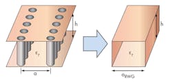
By forming them with SIW technology, it is possible to achieve excellent filter performance from small planar circuits. SIW transmission lines are created by forming two rows of metallized viaholes in a PCB substrate. The field distribution in a SIW transmission line is similar to that in a conventional rectangular waveguide.
Figure 2 shows the basic structure of an SIW transmission line. It has two rows of metallized viaholes on both sides of the substrate. The key design parameters for achieving a desired level of performance include the diameter of the viaholes, the separation between two successive viaholes, and the separation between the rows of viaholes. Such parameters are essential for designing low-loss SIW circuitry. To design an SIW circuit with low radiation loss, several conditions should also be met:
D < λg/5
and
b = 2D
where
a = the center-to-center distance between two parallel metallized viaholes;
b = the height of the substrate;
c = the speed of light in a vacuum;
d = the diameter of the metallized viaholes;
D = the periodic distance between two viaholes;
λg = the wavelength of the waveguide;
aRWG = the width of a dielectric filled metallic waveguide equivalent to the SIW
Parameter b should be as small as possible to minimize radiation losses. Parameter D, which also impacts the loss performance of an SIW circuit, will change according to b. The ratio of b to D is more critical in maintaining low radiation loss than the individual values of b and D.
When designing SIW transmission lines for a particular frequency range, the cutoff frequency, fc, is determined as a function of the width and length of the SIW structure. An SIW structure has highpass characteristics. It exhibits a transverse electromagnetic (TE) TE10 mode with dispersion characteristics—characteristics that are almost identical with the same mode of a dielectric filled rectangular waveguide with an equivalent width.
The effective width of an SIW structure is given by:
aRWG = a – (D2/0.95b)
while fc can be found from
fc = C/[2(εr)0.5 aRWG]
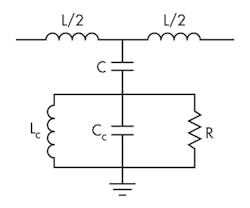
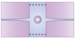
Figure 3 shows the layout of an SIW circuit with CSSRs etched in the top layer of a PCB substrate. Figure 4 depicts the layout of an SIW circuit with CSSRs etched in the bottom layer of the substrate. Since CSRRs are etched in the center of the top or bottom layers of the substrate—and they are mainly excited by the electric field induced by the SIW (as for TE10 mode)—this coupling can be modeled by connecting the capacitance of the SIW transmission lines to the CSRRs. Using this strategy, the lumped-element equivalent circuit for an CSRR-loaded SIW circuit is shown in Fig. 5.
As long as the electrical size of the CSRRs is small, the structures can be described by means of lumped elements. In these models, L is the SIW inductance and C is the coupling capacitance between the SIW and the CSRR. The resonator is described by means of a parallel tank,7, 8 with Lc and Cc being the reactive circuit elements and R accounting for loss.
Using this model, the transmission-zero frequency which nulls the shunt impedance was determined through simulations and measurements. To demonstrate the viability of the proposed technique, it was applied to the determination of the electrical parameters of a single-cell CSSR-loaded SIW circuit.
The structures of Figs. 3 and 4 were simulated for fabrication on RT/duroid 5880 circuit laminate material from Rogers Corp. The PCB material has a relative dielectric constant, ε r, of 2.22 at 10 GHz in the z axis (thickness) of the material. The material’s thickness, h, is 0.254 mm, and dissipation factor (loss), δ, is 0.002. The width of the access lines is 0.76 mm.
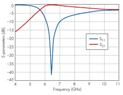
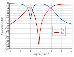
Figures 6 and 7 show the simulated scattering (S) parameters for the circuits depicted in Figs. 3 and 4, respectively. The circuit structures show similar characteristics, except that the circuit of Fig. 3 achieves higher stopband attenuation than the circuit of Fig. 4.
The single SIW CSRR cell shown in Fig. 4 was designed using a cell with outer-circle radius of 1.8 mm and inner-circle radius of 1.0 mm. To minimize losses, a microstrip feed was used to obtain maximum coupling between the SIW filter and the external feed line. By reducing the dimensions of the CSRR cell, the resonant frequency will increase.
The CSRR cell was loaded periodically onto the face of the SIW circuitry, but the edges of the CSRR cell were adjusted in size to achieve adequate bandwidth. As a result, their size has been slightly adjusted—to 1.7 mm for the outer-circle radius and 0.9 mm for the inner-circle radius—using the RT/duroid 5880 PCB substrate material.
Following simulation via the High Frequency Structure Simulator (HFSS) EM simulation software from ANSYS, the single cell CSRR was found to resonate at around 6.5 GHz, yielding negative effective permittivity at that frequency. Figures 6 and 7 show simulated results for the CSRR-loaded SIW structures of Figs. 3 and 4, respectively, from 4 to 10 GHz.
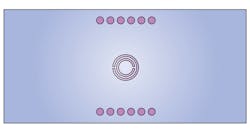
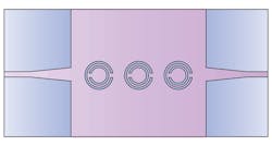
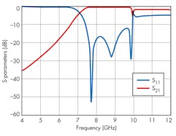
When CSRR cells are cascaded, as shown in Fig. 8, the SIW circuit exhibits bandpass behavior from 7.2 to 10.0 GHz with very low return and insertion losses. When two CSRR cells are added and aligned with the central CSRR structure, the resulting structure achieves wide bandwidth from 4 to 12 GHz as part of a bandpass response (Fig. 9).
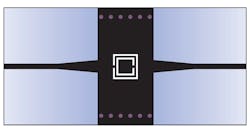
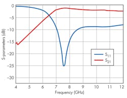
A SIW circuit with square CSRR cell was designed using a width of 3.6 mm for the outer ring and 2.0 mm for the inner ring (Fig. 10). A taper was employed to minimize losses by maximizing coupling between the SIW filter and the external line. Otherwise, the SIW circuit dimensions were the same as those for the SIW circuits with circular CSRR cells. The SIW circuit with square CSRR cell was simulated with HFSS software, with minimal reflections found around 7.4 GHz, when the effective permittivity of the CSRR cell is negative (Fig. 11).
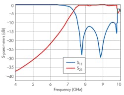
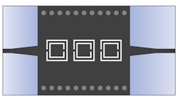
When square CSRR cells were cascaded (Fig. 12), a compact SIW circuit was achieved with bandpass response, with low return and insertion losses from 7.2 to 10.0 GHz. This compact bandpass filter has dimensions of 34 × 18 mm2 and is formed from three cascaded CSRR cells. It was simulated from 4 to 10 GHz with simulated results of -33.1-dB minimum return loss and 0.3-dB insertion loss at 8.8 GHz (Fig. 13).
The miniature CSRR-loaded SIW bandpass filter shows reasonable insertion and return losses from 7.2 to 9.8 GHz. This technology, of fabricating CSRR cells with SIW transmission lines on low-loss microwave substrate materials, shows great promise for the creation of compact bandpass filters at microwave frequencies.
Dr. Benmostefa Naima, Researcher
STIC Laboratory, Department of Electrical Engineering, Faculty of Technology, University of Tlemcen, Post Box 230, Pole of Chetouane, 13000 Tlencen, Algeria
References
1. F. Falcone, T. Lopetegi, J. D. Baena, R. Marqués, F. Martın, and M. Sorolla, “Effective negative-ε stop-band microstrip lines based on complementary split ring resonators,” IEEE Microwave Wireless Component Letters, Vol. 14, No. 6, June 2004, pp. 280-282.
2. S.N. Burokur, M. Latrach, and S. Toutain, “Analysis and design of waveguides loaded with split-ring resonators,” Journal of Electromagnetic Waves and Applications, Vol. 19, No. 11, 2005, pp. 1407-1421.
3. J. Bonache, I. Gil, J. Garcia-Garcia, and F. Martin, “Novel microstrip bandpass filters
based on complementary split-ring resonators,” IEEE Transactions on Microwave Theory & Techniques, Vol. 54, No. 1, January 2006, pp. 265-271.
4. J.B. Pendry, A.J. Holden, D.J. Robbins, and W.J. Stewart, “Magnetism from conductors and enhanced nonlinear phenomena,” IEEE Transactions on Microwave Theory & Techniques, Vol. 47, No. 11, November 1999.
5. J. Bonache, F. Martin, I. Gil, J. Garcia-Garcia, R. Marques, and M. Sorolla, “Microstrip bandpass filters with wide bandwidth and compact dimensions,” Microwave and Optical Technology Letters, Vol. 46, No. 4, August 2005, pp. 343-346.
6. Y. Cassivi, L. Perregrini, P. Arcioni, M. Bressan, K. Wu, and G. Conciauro, “Dispersion characteristics of substrate integrated rectangular waveguide,” IEEE Microwave and Wireless Component Letters, Vol. 12, No. 9, September 2002, pp. 333-335.
7. Jordi Bonache, Ignacio Gil, et al., “Novel Microstrip Bandpass Filters Based on Complementary Split-Ring Resonators,” IEEE Transactions On Microwave Theory& Techniques, Vol. 54, January 2006, pp. 265-271.
8.Xiaochuan Zhang, et al., “Microstrip Wideband Bandpass Filter Based on Substrate Integrated Waveguide (SIW),” IEEE International Symposium on Microwave, Antenna, Propagation, and EMC Technologies For Wireless Communications, 2007, pp. 209-211.

This file type includes high resolution graphics and schematics when applicable.
