RF/microwave components are often touted as “DC-coupled” products that are capable of transferring signals at 0 Hz. This is important for maintaining the integrity of certain digital and analog signals, especially in mixed-signal applications where a variety of different signal types might be in evidence. Unfortunately, many components are DC coupled in name only and fail the test when processing signals at 0 Hz.
One exception is the model PE42020 single-pole, double-throw (SPDT) surface-mount switch from Peregrine Semiconductor. With a frequency range of 0 Hz to 8 GHz, this rugged little switch is truly DC coupled and capable of handling a good amount of RF/microwave power for its size. It is well suited for applications in communications and test that combine DC, RF/microwave, analog, and digital signals.
This file type includes high resolution graphics and schematics when applicable.
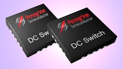
The PE42020 SPDT switch (see figure) is fabricated with UltraCMOS, Peregrine’s patented silicon-on-insulator (SOI) technology on a sapphire substrate. Peregrine’s HaRP technology, which essentially provides the performance of GaAs with the economy of silicon CMOS, supports high linearity with low harmonic distortion to help maintain signal integrity across wide frequency bandwidths.
The PE42020 switch, which is supplied in a 20-lead 4 × 4 × 0.85 mm QFN package, can be configured as an absorptive or open-reflective switch via single-pin control. It can handle maximum AC or DC voltage of ±10 V on its RF ports and is rated for maximum RF power of +30 dBm at DC and +38 dBm at 8 GHz.
This broadband switch features impressive total-harmonic-distortion (THD) specification of -84 dBc, measured at 1 kHz into a 300-Ω load. It exhibits low insertion loss between switched ports, at no more than 0.7 dB and typically 0.6 dB at 0 Hz; no more than 1.00 dB and typically 0.85 dB from DC to 3 GHz; no more than 1.30 dB and typically 1.00 dB from 3 to 6 GHz; and no more than 1.35 dB and typically 1.10 dB from 6 to 8 GHz. The isolation between ports varies with frequency, but is at least 46 dB and typically 48 dB from 0 Hz to 3 GHz; at least 35 dB and typically 37 dB from 3 to 6 GHz; and at least 30 dB and typically 34 dB from 6 to 8 GHz.
The switch can handle hot switching, when RF power is applied to the switch during the switching process, at input levels to +27 dBm when operating at positive and negative supply voltages of +15 V and -15 V (it is rated for slightly less hot-switching power at lower supply voltages). The switching speed, from 50% of a control signal to 10% or 90% of the RF signal, is 14 μs or less and typically 10 μs. The settling time, from 50% of the control signal to 0.05 dB of the final switched value, is 45 μs or less and typically only 35 μs.
The switch, which is designed for operating temperatures from -40 to +85°C, offers an input 1-dB compression point of typically +38 dBm from 40 MHz to 8 GHz. The input third-order intercept point (IP3) is typically +62 dBm at 836 and 1900 MHz, +61 dBm at 2.7 GHz, and +55 dBm at 4.8 GHz.
To assist adopters of the switch, the firm offers a switch evaluation board for the PE42020, complete with connections to 50-Ω transmission lines via SMA connectors. The evaluation board is constructed with four metal layers on low-loss printed-circuit-board (PCB) material, including 4350B circuit material from Rogers Corp. In addition to the RF connector, a 50-Ω through transmission line is available via SMA connectors for the purpose of de-embedding the losses of the PCB when evaluating the performance of the switch.
Peregrine Semiconductor Corp., 9380 Carroll Park Dr., San Diego, CA 92121; (858) 731-9400, FAX: (858) 731-9499
This file type includes high resolution graphics and schematics when applicable.
About the Author
Jack Browne
Technical Contributor
Jack Browne, Technical Contributor, has worked in technical publishing for over 30 years. He managed the content and production of three technical journals while at the American Institute of Physics, including Medical Physics and the Journal of Vacuum Science & Technology. He has been a Publisher and Editor for Penton Media, started the firm’s Wireless Symposium & Exhibition trade show in 1993, and currently serves as Technical Contributor for that company's Microwaves & RF magazine. Browne, who holds a BS in Mathematics from City College of New York and BA degrees in English and Philosophy from Fordham University, is a member of the IEEE.


