UWB Antenna Blocks Interference

This file type includes high resolution graphics and schematics.
Ultrawideband (UWB) communications offers great promise for transferring voice and high data rates over the frequency band from 3.1 to 10.6 GHz, provided that the components required for such systems can be designed and fabricated affordably. The antenna is one of the components which has attracted many designers since the United States Federal Communications Commission (FCC) opened that band for commercial use.1 The antenna presents numerous challenges, including broadband impedance matching and radiation stability in a relatively small structure that can be produced for low manufacturing cost.2
Related Articles
• UHF/UWB Antenna Supports Indoor Tracking
• Accurately Model UWB Antenna Pulses
• UWB Antenna Adds Two Notches
Over that broad UWB bandwidth, there are many applications that might represent interference for an UWB system, such as wireless-local-area-network (WLAN) systems operating from 3.3 to 3.6 GHz and from 5.725 to 5.825 GHz.3 Therefore, it is necessary to design UWB antennas with band-notched performance to eliminate potential interference. Signals from these two bands can be rejected by connecting two bandstop filters to an UWB antenna. But such an arrangement also increases the complexity and cost of the antenna. A more practical solution is to design an UWB antenna with band-notched characteristics. Such antennas have previously been designed,4-6 but owing to bulky structures,6,7 they are complex to design and manufacture.
As a possible solution, a simple, compact microstrip-fed UWB antenna with dual-band-notched characteristics at 3.4 and 5.8 GHz is proposed. It has a broad impedance bandwidth, owing to a modified ground plane with two fillets and a step-shaped slot. By etching a semicircular slot in the radiating patch, the first notched band from 3.3 to 3.6 GHz was achieved. To produce the second notched band from 5.725 to 5.825 GHz, a hook-shaped slot was cut in the ground plane.
In this dual-notch design, when one notch band varies, the other remains unchanged, due to the fact that the two slots are placed on different sides of the antenna and the coupling between them is weak. The band-notched antenna can be designed without retuning the dimensions of an original UWB antenna. Figure 1 shows the geometry and design of the proposed antenna, which was simulated and optimized by means of the High-Frequency Structure Simulator (HFSS) electromagnetic (EM) design software from Ansoft Corp.
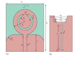
1. The diagram in (a) shows the geometry and configuration of the proposed dual-notched-band antenna while (b) shows part of the ground plane.
The antenna was printed on low-cost FR-4 PCB substrate material with relative dielectric constant, εr, of 4.4, loss tangent, δ, of 0.02, and thickness, h, of 1.6 mm. A circular patch with radius of R1 was printed on the top side of the substrate. This circular patch is connected to a microstrip line with width w. For a characteristic impedance of 50 Ω, the width of the microstrip line is fixed at 2.8 mm.
On the bottom of the substrate is a modified rectangular ground plane with two fillets and a step-shaped slot, which results in a broadened bandwidth. The step-shaped structure can be seen as an impedance transformer, and the fillets result in a smooth transition to the ground plane. These measures help to decrease discontinuities and reflections, allowing for good input impedance matching. Figure 2 shows the effects of the step-shaped structure and the fillets. The step-shaped structure affects the impedance over the full UWB frequency range. The fillets mainly influence the impedance at higher frequencies (8.5 to 11 GHz). The improved impedance matching is apparent when the modified ground plane is introduced.
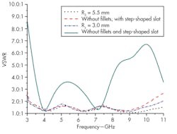
2. These curves show the effects on VSWR with frequency of the step-shaped slot and the fillets.
The semicircular slot in the radiating patch provides rejection of the 3.3-to-3.6-GHz band. By embedding the semicircular slot, a strong resonance results, leading to a sharp discontinuity of the input impedance and yielding the band-notched function. As detailed by ref. 8, given the dimensions of the band-notched feature, the notch frequency, fnotch, can be found from:
fnotch = c/2L(εre)0.5 (1)
where:
L = the total length of the slot;
εre = the effective dielectric constant; and
c = the speed of light.
For a dielectric substrate with thickness h, a microstrip line with width w, and relative permittivity of εr (as given by ref. 9), the effective permittivity can be found by Eq. 2:
εre ≈ 0.5[(εr + 1) + (εr – 1)(1 + 12h/w)-0.5 (2)
In the band-notched antenna design, the key parameters related to the 3.3-to-3.6-GHz notch are the width of the semicircular slot, d, the radius of the semicircular slot, R2, and the angle, θ. By changing these parameters, the frequencies of the notch and its bandwidth can be controlled. Figure 3(a) shows simulated VSWR for different values of d, with R2 and θ fixed. As the value of d increases, the notch frequency shifts lower in frequency and the bandwidth of the notch becomes wider. Similarly, the higher-frequency notch can be achieved by inserting the hook-shaped slot in the ground plane. Figure 3(b) shows that the second notch band can be modified by changing parameter k. When the higher-frequency notch is modified, the lower-frequency notch band remains almost unchanged.
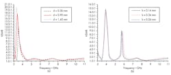
3. These plots show the effects of VSWR for (a) changes in d and (b) for changes in k.
Figure 4 shows the simulated and measured VSWRs for the proposed UWB antenna. Compared to the original design, the dual-band-notched design successfully blocks out the WiMAX/WLAN band and still exhibits good impedance-matching at other frequencies in the UWB band. Figure 5 is a photograph of the proposed antenna, connected with a 50-Ω SMA connector for excitation. The final parameters for the UWB antenna are a = 28 mm; b = 32 mm; R1 = 8.8 mm; R2 = 4.56 mm; R3 =5.52 mm; w = 2.8 mm, d = 1.22 mm; θ = 46 deg.; s1 = 11.9 mm; s2 =7.95 mm; k = 0.18 mm; g = 0.9 mm; t = 0.92 mm; m1 = 3.96 mm; m2 = 3.19 mm; m3 = 3.02 mm; n1 = 0.96 mm; n2 = 0.74 mm; and n3 = 0.45 mm.
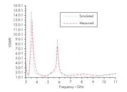
4. These plots compare measured and simulated VSWRs for the proposed UWB antenna.
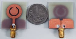
5. The fabricated UWB antenna is shown with its SMA launching connector.
According to Fig 2, three broadband resonators are formed with resonant frequencies centered at 4.2, 6.4, and 9.0 GHz. These resonances play important roles in broadening the antenna bandwidth. At the resonant frequencies, the VSWR should approach 1.0:1, so that reflections are minimal. Thus, the input impedance should be close to 50 Ω. Figure 6 shows the input impedance of the original UWB antenna without the band-notching structures.
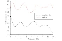
6. These plots show the real and imaginary part of input impedance for the UWB antenna without dual notched bands.
From Fig. 4, it is apparent that the notched bands are sharp. Due to the semicircular slot and the hook-shaped slot, two strong resonances occur, leading to impedance mismatching near the notch frequencies. It can be concluded that strong current distributions will exist along the two slots. Correspondingly, the input impedance should be considerably different than the characteristic impedance of 50 Ω. Figure 7 shows the input impedance of the dual-notched-band antenna, revealing that there is clearly a large impedance mismatch.
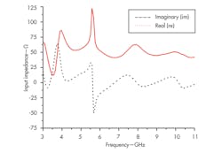
7. The real and imaginary parts of input impedance are shown here for the UWB antenna with dual notched bands.
Figures 8(b-d) show simulated surface current distributions for the proposed dual-notched-band antenna, with simulated current distributions for the original UWB antenna without notches shown in Fig. 8(a). As the original UWB antenna shows, the currents concentrate mainly on the lower patch and the microstrip line. As Fig. 8(d) shows, at 8.7 GHz, the current flows mainly along the microstrip line and the lower patch, while current flow is weak around the two slots. This explains why the semicircular slot and the hook-shaped slot have little effect on the UWB antenna performance across most of its operating frequency range.
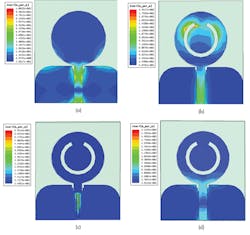
8. These plots show simulated current distributions at different frequencies (a) 8.7 GHz for the UWB antenna without notched bands; (b) at 3.6 GHz for the UWB antenna with dual notched bands; (c) at 5.6 GHz for the UWB antenna with dual notched bands; and (d) at 8.7 GHz for the UWB antenna with dual notched bands.
At 3.6 GHz, the majority of the current flow is around the semicircular slot. At 5.6 GHz, the current is concentrated mainly on the hook-shaped slot. This is consistent with the strong resonances and the impedance of the two slots being nearly zero in the two notched bands. Based on the current distributions, the lower patch plays a major role on current distribution, while current is minimal on the top of the patch, implying that the top of the patch might be removed for a compact antenna design.
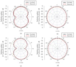
9. These plots show measured and simulated radiation patterns for the proposed antenna: (a) X-Z plane (E-plane) patterns at 4.4 GHz; (b) Y-Z plane (H-plane) patterns at 4.4 GHz; (c) X-Z plane (E-plane) patterns at 6.0 GHz; and (d) Y-Z plane (H-plane) patterns at 6.0 GHz.
Figure 9 shows the simulated and measured H-plane and E-plane radiation patterns of the proposed antenna at 4.4 and 6 GHz. Figure 10 shows three-dimensional (3D) radiation patterns at 6.4 GHz. The patterns in the magnetic (H) plane are omnidirectional, while radiation patterns in the electric (E) plane are bidirectional. These radiation patterns are quite stable. Figure 11 shows the simulated and measured maximum gain of the proposed antenna. Note that the gain drops significantly at the notched bands. However, the proposed antenna shows good gain performance at other frequencies across the UWB band.
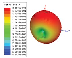
10. These plots show 3D radiation patterns at 6.4 GHz.
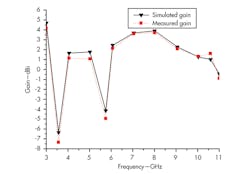
11. Measured and simulated gain are plotted here as a function of frequency.
Since UWB communications systems employ pulsed signals, stable group delay is desirable. Figure 12 shows the group delay of the original antenna without the dual notched bands and the antenna with the dual notched bands. Without the notched bands, the group delay is constant. With the notched bands, the group delay is much higher. The proposed antenna achieves good phase linearity and provides the performance characteristics that make it a good candidate for UWB systems.
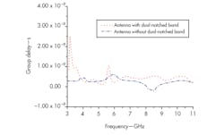
12. Group delay is plotted here for the original UWB antenna without notched bands and for the UWB antenna with dual notched bands.
Kun-Long Min, Ph.D
Department of Electromechanics Engineering, Northeast Forestry University, Harbin 150040, People’s Republic of China
Jia-Wei Zang, Professor
School of Information and Electronics, Beijing Institute of Technology, Beijing 100081, People’s Republic of China; e-mail: [email protected].
Wen-Long Song, Engineer
Department of Electromechanics Engineering, Northeast Forestry University, Harbin 150040, People’s Republic of China
Acknowledgements
This work was supported by the National Natural Science Foundation of China (grant No. 31270757), Program for New Century Excellent Talents in University (NCET-09-0279), the Specialized Research Fund for the Doctoral Program of Higher Education of China (20110062110002), and Fundamental Research Funds for the Central Universities (DL12DB05).
References
1. “First report and order in the matter of revision of Part 15 of the commission’s rules regarding ultra-wideband transmission systems,” Federal Communications Commission, Washington, DC, ET-Docket 98-153, 2002.
2. Y.C. Lin and K.J. Hung, “Compact ultrawideband rectangular aperture antenna and band-notched designs,” IEEE Transactions on Antennas & Propagation, Vol. 54, November 2006, pp. 3075-3081.
3. S.W. Su, K.L. Wong, and C.L. Tang, “Band-notched ultra-wideband planar monopole antenna,” Microwave and Optical Technology Letters, Vol. 44, February 2005, pp. 217-219.
4. Y.F. Weng, S.W. Cheung, and T.I. Yuk, “Compact ultra-wideband antennas with single band-notched characteristic using simple ground stubs,” Microwave and Optical Technology Letters, Vol. 53, No. 3, March 2011, pp. 523-529.
5. Chih-Yu Huang and En-Zo Yu, “A slot-monopole antenna for dual-band WLAN applications,” IEEE Antennas & Wireless Propagation Letters, Vol. 10, 2011, pp. 500-502.
6. W.-S. Lee, K.-J. Kim, D.-Z. Kim, and J.-W. Yu, “Compact frequency-notched wideband planar monopole antenna with a L-shape ground plane,” Microwave and Optical Technology Letters, Vol. 46, August 2005, pp. 340-343.
7. Mohammad Yazdi and Nader Komjani, “Design of a band-notched UWB monopole antenna by means of an EBG structure,” IEEE Antennas & Wireless Propagation Letters, Vol. 10, February 2011, pp. 170-173.
8. J. Han and W. Ding, “A novel printed monopole antenna for dual-band WLAN application,” International conference on Wireless Communications & Signal Processing, November 2009, pp. 13-15.
9. Q.X. Chu and Y.Y. Yang, “A compact ultra-wide band antenna with 3.4/5.5GHz dual band-notched characteristics,” IEEE Transactions on Antennas & Propagation, Vol. 56, No. 12, December 2008, pp. 3637-3644.
This file type includes high resolution graphics and schematics.
