How to Use Lumped Constants in Microwave Circuit Design
March, 1968
The latest microelectronic techniques now make possible the design of lumped-constant circuits at microwave frequencies. Whereas a few hundred megacycles appeared to be the limit for lumped-constant “conventional” circuits in the past, new methods extend this to over 1 Gc.
The usual criteria for the use of lumped components is that the largest linear dimensions of such components should not exceed 1/100 wavelength. So-called “conventional components” usually fail this test at less than 300 Mc.
At 1.0 Gc, the free-space wavelength is 30 cm. For a medium with a dielectric constant of four, the wavelength reduces to 15 cm. In this medium, the maximum linear dimension of a component (based on 1/100 λ) is 1.5 mm, or about 0.060 in.
Fortunately, the new thin-film components meet the spatial requirement in the lower microwave region. Although tin-film inductors, for instance, are only practical into the nanohenry range, needed inductance above 300 Mc is usually low enough to make such inductance useful.
This file type includes high resolution graphics and schematics when applicapable.
Criteria for thin-film components
By imposing the spatial restrictions on thin-film components, attainable values at microwave frequencies are as follows:
Resistors: The value of a thin-film resistor is
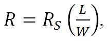
where
RS = specific resistance of a film in ohms per square,
L = resistor length, and
W = resistor width.
The specific resistances generally used are in the order of a few hundred ohms per square (e.g., 200), and usable line widths can be as small as 0.001 in. Thus, thin-film resistors for use at microwaves can be fabricated in the range from 4 to 400,000 ohms.
Capacitors: The value of simple two-plate thin-film capacitor is
C = CSA,
where
CS = specific capacitance in picofarads per square mil, and
A = capacitor area.
The specific capacitance is limited by the breakdown voltage desired for the capacitor. For small-signal semiconductor circuits, 50 V is usually adequate; for this breakdown voltage, a specific capacitance of 0.05 pF per square mil is not difficult to achieve. The smallest practicable capacitor area is 1 square mil. Thus, thin-film capacitors for use at microwave frequencies range from 0.05 to 125 pF.
Inductors: For flat spiral thin-film inductors, the inductance is approximately
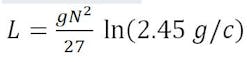
where
L = inductance in microhenries,
N = number of turns,
g = mean coil diameter in inches, and
c = the radial coil depth in inches, assuming the conductor width equals the conductor spacing.
In a 0.050-in. dia circle, the maximum inductance obtainable is 125 nH. The specific resistivity of thin-film conductors is normally about 0.05 ohms per square, from which it follows that the inductors will have Qs of about 20. The minimum inductance for a 0.050-in. conductor pad is on the order of 0.2 nH.
The advantage of using lumped constants at the lower microwave frequencies is essentially one of size. If a distributed technique is used (such as microstrip on alumina) each distributed element will be about a quarter-wavelength on a side. Alumina has a dielectric constant of nine; thus, a quarter wavelength at 1.0 Gc is about 1.0 in. A single-stage microstrip amplifier will consequently occupy an area of about 2 in.2. If thin-film lumped components on a glass substrate are used, a two-stage amplifier occupies an area of only about 0.08 in.2. Thus the reduction in size is appreciable.
Transistor parameters
This file type includes high resolution graphics and schematics when applicapable.
Transistors are obtainable in all types of packages ranging from TO-18 cans to bare uncased chips. Several manufacturers supply units in TO-50 cans or other packages compatible with strip-line or microstrip circuitry. Data on such transistors for use at microwave frequencies are often minimal. Although some manufacturers supply y-parameter curves over an extended frequency range, such parameters are generally given for cased units only and do not reflet the characteristics of the bare chips. The packaged transistor parameters, however, are not bad approximations to determine device performance when wire bonding the bare chips to substrates, because wire lengths are uncased or in a can.
Design example
A two-stage transistor amplifier, using lumped-constant passive components was designed to illustrate the techniques involved.
A type TI 2N3570 transistor was selected on the basis of cost and availability, and good datasheet information covering pertinent characteristics at the frequency of interest, 1.0 Gc. Parameters for a TO-18 cased transistor are given on the data sheet, but an assumption was made that the chip bonded to a thin-film substrate exhibits similar y parameters.
The amplifier design is considered an extension to the microwave region of lower frequency design techniques. Thus, the Linvill method was chosen as a starting point. This design technique consists basically of using transistor two-port parameters (in this case, the y or admittance parameters) to determine values of gain for different input and output terminations. After determining the terminations required for a specific gain, matching networks are designed to conjugately match the transistor with its input source and output load impedance.
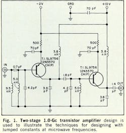
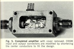
The completed circuit of the two-stage amplifier is shown in Fig. 1. The power-supply by-pass capacitors are the largest possible for the available space on the thin-film substrate.
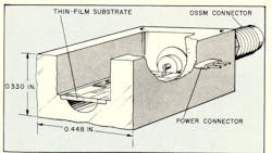
In packaging the amplifier, the holder or box was designed with the following criteria in mind:
- small size,
- adequate grounding of the thin-film substrate,
- minimum length of signal leads, and
- reduction of stray capacity.
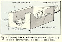
The box is machined from solid brass and accepts the rf connectors directly. The thin-film substrate rests on machined ledges, and the ground plane around its periphery is then soldered to the ledge. This operation is performed by heating the box to a controlled temperature and flowing solder around the ledge. Excellent electrical and mechanical contact is made.
Design example (continued)
This file type includes high resolution graphics and schematics when applicapable.
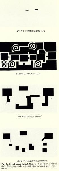
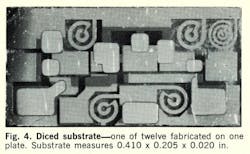
All layers are vacuum evaporated on a glass substrate with a dielectric constant of four. The bottom conductor layer is gold, 2200 Å thick, with a specific resistance of 0.1 ohm per square. The resistive layer is chromium, 300 Å thick with a specific resistance of 200 ohms per square and a TCR of ± 110 ppm. The third layer is silicon monoxide, 12,000 Å thick, with a specific capacitance of 0.030 pF per square mil. This serves both as the capacitor dielectric and as resistor protection. The last layer is aluminum, 2000 Å thick, with a specific resistance of 0.1 ohm per square. Twelve substrates are fabricated on one plate and then diced (One of the diced substrates is shown in Fig. 4 and measures 0.410 x 0.205 x 0.020 in.). Both ac and dc tests are then performed.
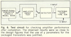
Amplifier performance
The amplifier test circuit is shown in Fig. 6. OSSM-to-N adaptors are used at the amplifier terminals. All impedances are 50 ohms.
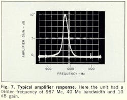
A number of amplifiers have been made at different frequencies, by bonding to different points on the inductors. The lowest center frequency attainable was 650 Mc. A typical response for an amplifier with a center frequency of 987 Mc, a 40-Mc bandwidth, and 10-dB gain, is shown in Fig. 7. There was no saturation with 1 mW rf input at 120 mW power dissipation. The observed results were so close to the design figures that the use of y parameters for the packaged transistors seems justified.
In system use, the amplifier would not be packaged by itself. Thus, the volume occupied by the amplifier substrate, with attached chips would be only 0.0008 in.3.
Conclusion
The lumped-constant microelectronic approach appears attractive at the lower microwave frequencies. Its advantages, compared to microstrip circuitry, are that of small size and the use of familiar design at lower frequencies. Although circuits cannot be breadboarded in conventional fashion, the Linvill design technique, in combination with precise substrate fabrication, yields operating parameters quite close to the design values. The present difficulty in obtaining ac parameters for uncased transistor chips does not appear serious and, in any case, it will probably be possible to obtain this information in the near future.
This file type includes high resolution graphics and schematics when applicapable.
