Microwave Diodes… Why a Schottky-barrier? Why a Point-contact?
March, 1968
Since World War II, the point-contact diode has been the most useful converter of microwave signals to lower frequencies. Now, a new device—the Schottky-barrier diode—is claimed to offer improved electrical efficiency and higher reliability for this and other applications. A comprehensive evaluation of both devices leads to the conclusion that each has its place in microwave design. Here are the facts.
Construction differences
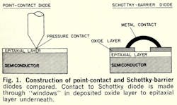
Both the point-contact and Schottky diodes consist of a die of semiconductor material on which an epitaxial layer is deposited. The point-contact diode uses a metal whisker to make pressure contact against the epitaxial layer, forming the rectifying junction. The Schottky diode has an additional oxide layer deposited over the epitaxial layer. A “window” is photo-etched through the oxide layer to the epitaxial layer through which a metal contact is then deposited. Thus, the main difference between these devices is the pressure contact used in the point-contact diode compared with the deposited contact in the Schottky diode. The pressure contact in the point-contact diode can damage the junction, depending on the amount of pressure exerted on the contact, while the Schottky diode lends itself to better control and more repeatable fabrication.
Mode of operation
Detection and mixing
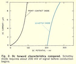
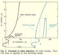
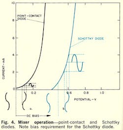
The mixer diode can be treated in somewhat the same manner (see Fig. 4). Conduction for the Schottky diode occurs only after about 300 mV, while the point-contact diode will operate as an efficient mixer, with a bias of only about 200 mV p-p and a signal of 40 mV p-p. Also, if the LO drive is increased to a point where the Schottky diode is driven into forward conduction, it also becomes an efficient mixer. The use of a dc bias, as shown in Fig. 4, permits the Schottky diode to operate with less LO drive. Use of dc bias also enables the point-contact diode to operate with lower drive.
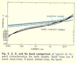
Dc characteristics
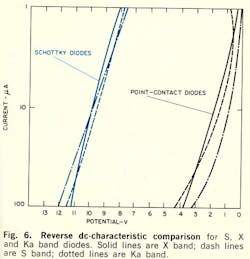
A comparison of the reverse characteristics of the two types is shown in Fig. 6. The point-contact diodes have very low reverse voltage drops for any given reverse current as compared to the Schottky diodes. Although not generally specified, point-contact diodes typically have 3-V PIV’s at 100 μA; whereas, Schottky diodes are generally specified as 10 μA and a 7-V PIV. At 100 μA, the Schottky PIV would be about 12 V or four times that of a point-contact diode.
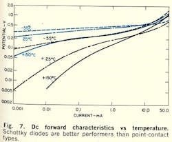
A comparison of forward characteristics with temperature is shown in Fig. 7. At currents of 1 mA or more, the change vs. temperature is much less than at currents of 100 μA or less. This is because at higher currents, variation dude to internal heating caused by forward conduction I-R drop tends to swamp out variations due to ambient temperature. Although the changes for Schottky diodes are less than those for point-contact units, they still follow the same general pattern.
Comparison of reverse characteristics vs. temperature is shown in Fig. 8. The change in PIV at 150-deg. C is extreme for the point-contact diodes—becoming 1/3 its room temperature value—whereas, the change is only about 10% for the Schottky diode.
Comparison of rf characteristics
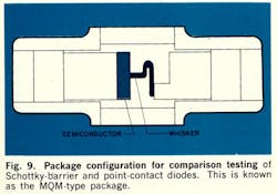
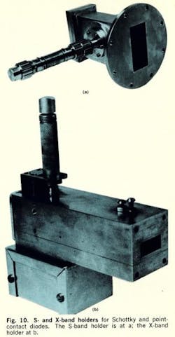
A cross section of the diode, as it appears when packaged, is shown in Fig. 9. The unit consists of two metal ends and a glass body. The glass is sealed to the kovar ends, thus making a true hermetic seal. Length is approximately 0.2 in., body diameter, 0.08 in. and metal-end diameter 0.062 in.For test purposes, each diode was placed in a holder matched to the diode’s impedance at spot frequencies. Although the MQM package is suitable for strip-line and miniature packages, the holders used for testing were selected to mate with standard test equipment. Holders for S-band and X-band are shown in Fig. 10.
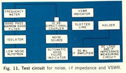
The test set-up for measurements at both S- and X-band is shown in Fig. 11. A low-noise klystron was used. Since the measurements were made in a single-diode mixer, it was essential to have a narrow band-pass filter to ensure rejection of the LO sideband noise. The 30-Mc amplifier was matched to the resistance and capacitance presented by the diode holder combination.
Mixer characteristics
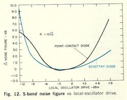
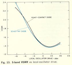
The change in noise figure vs. local-oscillator drive for S-band diodes is shown in Fig. 12, and is similar to the X-band diodes. The Schottky diode has the best performance over the range from +6 to +3 dBm, similar performance from 0 to -6 dBm, and marked degradation beginning around -10 dBm. The point-contact diode gives better noise figure in the -12 dBm range.In Fig. 13, which shows VSWR vs. LO drive, the two diodes are comparable until the drive drops to -9 dBm, beyond which the Schottky diode deteriorates faster than the point-contact device.
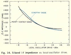
As shown in Fig. 14, the change in i-f impedance vs. LO drive is comparable for both diodes. The use of dc bias will improve the characteristics for both diodes beyond -12 dBm.
The change in noise figure vs. temperature for both diodes at S and X-bands is shown in Fig. 15. Over the range from -55-deg. C to +150-deg. C, the Schottky diode changes 1 dB at S band while the point-contact diode changes about 5 dB. Most of this change occurs over the high temperature range. Somewhat better performance is obtained with both diodes at X-band, as shown.
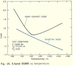
The VSWR vs. temperature response for S-band diodes, similar to that for X-band diodes, is shown in Fig. 16.
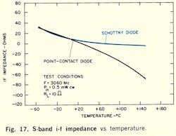
Variation in i-f impedance with temperature for S-band diodes is shown in Fig. 17. The point-contact device varies about 100 ohms. Similar results were obtained on X-band diodes.
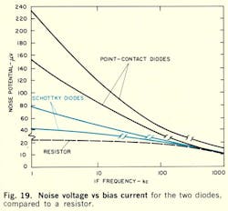
Another concern in mixer performance is low-frequency noise introduced either by LO or dc bias. Noise voltages obtained at various i-f frequencies for Schottky, and point-contact diodes, as compared to a resistor, are shown in Fig. 19. The two curves for each type diode are for two different bias levels. In each case, the Schottky-diode noise voltage at 1 kc is better than the point-contact by a factor of 3, with the two diodes reaching a comparable condition at 1000 kc.
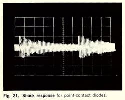
The response obtained while shocking typical point-contact diodes is shown in Fig. 21. The ringing effect is caused by the change in pressure exerted on the contact as the whisker vibrates, thus causing a change in the diode’s barrier resistance.
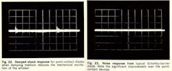
The waveform in Fig. 22 is obtained for a typical point-contact diode which has been filled with a damping medium to reduce the mechanical oscillation of the whisker. Note the drastic reduction in microphonics. Noise from a typical Schottky diode is shown in Fig. 23. The improvement over the point-contact diode is apparent.As a detector
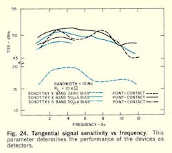
Results of this evaluation are shown in Fig. 24, which clearly shows the comparison between X-band Schottky and point-contact diodes. When operating without dc bias, the Schottky diodes are approximately 30 dB poorer in this test than the point-contact units. This would be expected, because the Schottky diodes are non-conducting at low bias levels. With dc bias, the Schottky diode is comparable to the point-contact unit.The use of dc bias changes the video impedance and noise characteristics of the diodes. Point-contact diodes without bias have video impedances of approximately 4 kΩ to 100 kΩ. Schottky diodes are in the 10’s of megohms. With 50 μA dc bias, point-contact diodes have video impedances in the range of 1.5 to 4 kΩ, whereas the Schottkys are in the range of 5 to 6 kΩ. The video impedance, coupled with the capacitance of the holder-amplifier combination, has a critical effect on the plus fidelity due to the charging time-constant of the circuit. Bias on point-contact diodes will result in better pulse fidelity than with Schottkys because of the lower video impedance.
The noise generated within the diode by the dc bias is lower in the Schottky than in the point-contact device. However, Schottky diodes with very low capacitances have shown high noise. This is attributed to the high RS associated with low capacitance.
Temperature runs of both diodes show the Schottkys to be more stable with temperature variation, while the point-contact tangential signal sensitivity varied 3-5 dB at high temperatures.
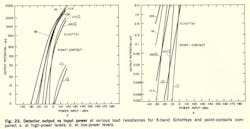
Families of curves, showing voltage output vs. power input and load resistance for both point-contact and Schottky diodes, are shown in Fig. 25. The higher peak inverse voltages of the Schottkys, as compared with the point-contacts, are evidenced by their higher open-circuited voltage. The higher starting voltage of the Schottky diode, compared to the point-contact, is also evident.
The future of the Schottky diodes
What does the future hold in store for the Schottky diode?
At present, these diodes are limited to an upper frequency of about 40 Gc. Research and development now in process will push this limit higher. The Schottky diode has the potential of being the circuit designer’s “dream” diode—the active junction with no package.
Burnout comparison
Continuous power seldom exceeds ratings in most applications since microwave mixer diodes operate with a local-oscillator power input of a few mW, well within their rating. As a detector covering a wide dynamic range, the diode’s capability may be exceeded at the high-power inputs. In practice, this problem can be eliminated by adding enough attenuation to protect the diode at the maximum input-power level while accepting reduced signal output at low-input power.Burnout is a major cause of operation failure of microwave diodes. Burnout (for this discussion) is defined as catastrophic failure such as an open or short circuit or a 3-dB degradation in electrical performance. Burnout may be due to excessive energy (continuous or transient) dissipated in the diode.
It is more difficult to protect against transient energy. Two major causes of excessive transient energy are TR tube leakage and high-energy signal pulses.
Using the same MQM packaging configuration, burnout comparison of Schottky and point-contact S- and X-band diodes is shown in Fig. 26. The tests were performed by subjecting groups of diodes, one at a time, to a single pulse from a Torrey line. The charging voltage was increased with successive pulses until the diodes were destroyed.
The S-band Schottky diodes were better at higher voltage levels than the point-contact diodes, as shown at α. The X-band Schottky diodes were better than the point-contact diodes at the lower voltage levels, as shown at b. X-band devices withstand less voltage than the S-band diodes because of the smaller junction of the higher frequency diodes.
The Schottky diodes appear better at lower charging voltages at S-band, as shown in Fig. 27a. At X-band, the point contact diodes appear better, as shown at b. These curves point out the significance of the application and the test procedure in evaluating diode burnout resistance.
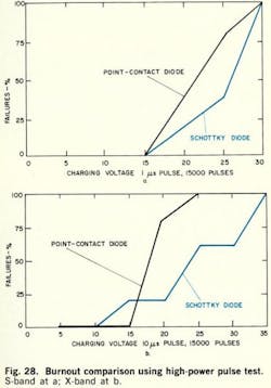
Another type of pulse burnout of interest is that encountered with high-powered pulses in the order of 50 ns to a few ms duration. Such pulse widths might be experiences by a diode in a video receiver. The peak pulse power is the significant factor in causing diode burnout. In testing for this, Schottky diodes are superior at both the 1.0- and 10.0-ms pulse widths, as shown in Fig. 28.
Cw power capability
The ability to withstand cw power is of interest in some applications of microwave diodes, such as in power monitors on an intermittent basis or in harmonic generators on a continuous basis.
Cw power-capability tests were performed by applying power to the group of diodes at a sequence of increasing power levels for short periods of time until the diodes were destroyed or the maximum power of the test circuit was reached. X-band point-contact and Schottky diodes were mounted in a holder one at a time. Each diode was matched to the power source at each power level, in order to get maximum power dissipation in the diode. Two different diode loads were used.
With the 10-kΩ load, point-contact diodes started to fail at 640 mW while Schottky diodes showed no failures up to 800 mW. With the 10-Ω load, Schottky didoes showed changes at 160 mW while the point-contact diodes showed no change up to 800 mW.
These results can be understood in terms of the diode characteristics. With the 10-Ω load, the forward current will be greater in the Schottky diode because of its lower series resistance; and consequently, the power dissipated in the device will be higher at the same input power level. With the 10-kΩ load, less forward current will exist and less power will be dissipated in the diode.
However, the voltage built up across the diode in the reverse direction will be much higher with the 10-kΩ load; and the point contact diode with its much lower PIV characteristics will start to conduct much sooner in the reverse direction with subsequent diode damage. The better PIV characteristics of the Schottky diode will also be an advantage in some applications, such as in video detector systems, where a possibility of pulse leakage from nearby transmitters exists.
Schottky didoes withstand burnout better than point-contact diodes. The amount of superiority demonstrated varies from one type of test to another and is a reflection of the problems of test instrumentation. The experimental data support the theoretical superiority of a junction device, with its greater uniformity, over a point-contact device which depends on a pressure contact between tungsten and silicon for rectifying junction.
Environmental and fabrication considerations
These tests prove that Schottky diodes are suitable for severe military and space environments. Point-contact devices, likewise, withstand the same degree of mechanical and thermal stress as the Schottky diode.Since most microwave diodes will be used in military equipment with rugged service environments, it is necessary to know the ability of microwave devices to withstand severe environmental stress. Schottky didoes will withstand high mechanical and thermal stresses as demonstrated by tests performed under the standard conditions of MIL-STD-750 for semiconductors. Schottky didoes will withstand mechanical stresses of 20 G vibration, 1500 G shock, and 20,000 G acceleration. Schottky diodes will withstand temperatures cycling from -65 to 150-deg. C. No deterioration was evident after 1000-h storage at 150-deg C.
Schottky diodes have two fabrication advantages over point-contact devices that result in greater uniformity and, therefore, in greater reliability in large-scale production. Schottky diodes are made by forming a large number of junctions on a single wafer of semiconductor material. This process, which is one used for the majority of semiconductors, is capable of close control. These junctions can be measured for dc characteristics and capacitance while still on the wafer or in chip form, which results in tight process control. Point-contact devices, however, are made by a pressure contact between the semiconductor and the metal contact. This fabrication method results in significant variation in dc characteristics from device to device. Furthermore, these dc characteristics can only be measured in the finished assembly.
The Schottky diode should be much more uniform in high-volume production than the point-contact diode. Variations in package materials and processes can be separated from semiconductor variations so that impedance variations from device to device should be much less with Schottky diodes.
Using Schottkys in circuits
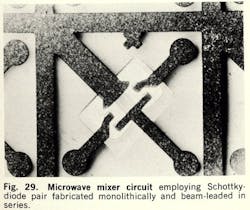
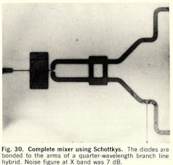
The complete mixer is shown in Fig. 30. Here the diodes are bonded to the arms of a quarter-wavelength branch line hybrid, and the i-f signals are combined at the center top of the diode pair and fed out through a low-pass filter. This mixer has successfully performed at X-band with a noise figure of 7 dB.
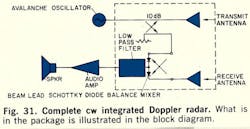
As an illustration of other applications of this technique, a demonstration model of a cw integrated Dopplr radar has been fabricated as shown in Fig. 31. It consists of a 9.5-Gc avalanche-diode oscillator, which serves as transmitter and local oscillator (the system operates at zero i-f frequency), a directional coupler, separate transmit and receive antennas, a Schottky-diode balanced mixer, low-pass filter, audio amplifier and loud speaker. A moving target produces a Doppler-shifted return signal, which is down converted to an audio frequency, amplified and fed to the speaker.
