Microwave Transistor-Parameter Trade-offs in Circuit Design: Part 2
October, 1967
Although dc parameters, as covered in Part 1 of this series, give a great deal of information about a transistor for use at microwave frequencies, rf parameters are important, too. The parameters to be considered are hfe, GPE, η, rf BVCEO, and VCE(SAT). Each will be defined and discussed in turn.
This file type includes high resolution graphics and schematics when applicapable.
Hf forward-current transfer ratio (hfe)
The high-frequency common-emitter forward-current transfer ratio of a transistor is the ratio of the short-circuit output current divided by the input current. This is the high-frequency Beta of the device. The theoretical curve of current gain vs frequency is shown in Fig. 1 and is very closely approached in practice.
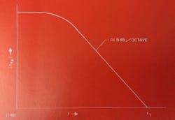
Fig. 1. Theoretical curve—hfe vs f.In practice, the high-frequency current transfer ratio varies with frequency in a manner closely approximating the theoretical curve shown.
The frequency at which hfe is 1 (or 0 dB) is usually considered as being fT, the current-gain times bandwidth of the transistor. Parameter fT is usually estimated by multiplying hfe by the frequency of measurement. In practice, however, measured hfe times frequency of measurement does not give fT – especially for high-power rf transistors. The external hfe is not necessarily that of the internal structure and thus is not always an exact measurement or estimate of fT. The difference is cause by the division of input current between the input resistance depends upon the emitter inductance and whether there is resistor stabilization in the emitter structure. Thus, the measured hfe may not be the actual internal gain of the structure. Although external current gain is important, in estimating power gain it is the internal current gain that should be used. This is especially so if emitter inductance is to be neglected or if any emitter resistance will otherwise be used in the power gain formula. All transistor manufacturers’ data sheets specify hfe as the external measurement. However, the internal (current) gain-bandwidth product can be somewhat higher depending upon device type and packaging.
Parameter hfe determines many circuit capabilities as well as some of the dc transistor parameters. It is not a measure of power gain, because base resistance (which can be established somewhat independently of hfe or fT) also enters into determination of power gain.
Input and output admittances
To design adequately a high-frequency power-transistor circuit, the approximate impedances to which the input and output must be matched need to be known. In effect, it is the large-signal impedances that are important. These are difficult to determine with available measuring equipment, but accurate measurement techniques have been established. At present, mostly small signal parameters are specified. These place the circuit design in the right ball park for the large-signal impedance values, which are now being specified on some manufacturers’ data sheets.
Common-emitter admittances are normally given in the transistor specifications such as input admittance y11e (the input admittance with output short-circuited) and output admittance y22e. Typical forward-bias curves for these small-signal values are shown in Fig. 2. The large-signal input resistance will be less than the small-signal value. Thus, the circuit designer must compensate for this. The large-signal output admittance will be closer to the small-signal value if the latter is measured at less than the large-signal circuit operating voltage.
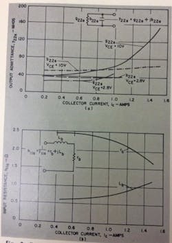
Fig. 2. Typical forward-bias curvesfor small-signal values of common-emitter admittance and large-signal input resistance. Curves were obtained on a type ITT-3TE440 transistor at 400 Mc.
Typically, the small-signal measurement of y22 at 10 V will agree closely with the large-signal value at around 28 V. Sometimes, the equivalent series circuit input resistance and reactance are given rather than the shunt values.
Common-emitter power gain (GPE)
This file type includes high resolution graphics and schematics when applicapable.
The large-signal common-emitter power gain, GPE, is the ratio of the output power, POE, to the input power, PIE, in a common-emitter power-gain circuit. Most specifications give the PIE range for a given POE and supply voltage. Power gain typically decreases as the temperature of the transistor increases at high frequencies. The reverse may be true using a high-frequency transistor at low frequency. It is also a function of the power-output level and the transistor’s dc parameters. A typical dependence of power gain on power output is shown in Fig. 3. The closer the power output design center is to the transistor’s saturated power output, the greater the fall-off in power gain with increased drive, and the greater the variation from transistor to transistor.
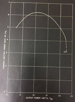
Fig. 3. Typical dependence of power gain on output power from microwave transistors.
Power gain is normally measured with the input and output simultaneously matched for maximum power gain. Occasionally, some mismatch is allowed to improve efficiency. Power gain is typically specified in a narrow-band tuned circuit. Broader bandwidth power gain would be somewhat lower.
Power gain theoretically decreases with increased frequency at 6 dB per octave. In practice, it decreases slightly faster than this. How power gain typically varies with frequency is shown in Fig. 4. Theoretically, the power gain is 1 (0 dB) at fmax (maximum frequency of oscillation). At this point, all of the output power would have to be fed back to the input of the device to sustain oscillation. In good present-day devices, fmax can be considerably higher than fT, and thus significant power gain can be obtained at a frequency above fT. This is because power gain is proportional to fT/rb. Base resistance is consequently a major factor in high-frequency performance.
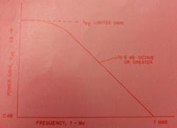
Fig. 4. How power gain decreases with frequency—a theoretical curve.
Collector-circuit efficiency (η)
Collector-circuit efficiency is an important parameter because it involves the power consumption of the power amplifier. Collector deficiency is defined by:
Assuming that the amplifier stage has reasonably high-power gain, the collector-circuit efficiency is then very nearly the over-all efficiency which is defined:
For a given tuned circuit, η varies with power output as illustrated in Fig. 5. Collector efficiency can very much be a function of the circuit design, but it also relates to some transistor parameters.
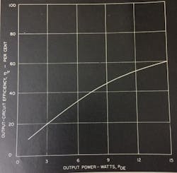
Fig. 5. Collector-circuit efficiency as a function of output power for a typical microwave transistor (ITT3TE440) at 400 Mc. Vcc = 40 V.
Rf breakdown voltage
This file type includes high resolution graphics and schematics when applicapable.
Initial studies by James Janky, at ITT Semiconductors Applications Engineering Department in September, 1966, show that the rf breakdown voltage of a transistor is higher than its dc value (in a CEO or CEX mode) and can approach its BVCBO value at high frequencies. Attempts to measure this value may be accomplished by applying rf directly to the collector and measuring the result. The result is very dependent on the circuit in the base and the capacitive current through COB. A circuit, which leaves the base open at rf, tends to approximate the typical condition of an amplifier circuit but will give much lower breakdown values than if the Cob current is shorted at the base (BVCES) which will measure closer to BVCBO at rf.
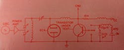
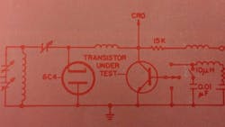
Fig. 6. Rf breakdown test circuit.
A simple, straightforward rf breakdown test circuit is shown in Fig. 6. The transistor is normally in the OFF condition; a reverse bias is applied to the collector; and rf peak voltages are applied to the unit until breakdown occurs.
The BVCEO of the 2N3375 with 40 V bias is shown in Fig. 7. Only a 10 percent increase is apparent here. BVCES will be considerably higher.
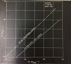
Fig. 7. Dc vs rf breakdown voltage for transistor 2N3375 operating at 130 Mc with 40-V bias.
Transistor epitaxial thickness and basewidth are important factors because these affect the avalanche multiplication factor. Table 1 gives the range for other device types.
Table 1: Dc and rf breakdown-voltage comparison for typical microwave transistors
|
Transistor type |
DC BVCEO (Volts) |
RF BVCEO @100 Mc (Volts) |
|
2N3866 |
34 |
50 |
|
2N3632 |
50 |
92 |
|
3TE160 |
75 |
96 |
|
3TE250 |
100 |
130 |
|
3TE350 |
60 |
62 |
Much work must yet be done to determine how the actual operating-circuit breakdown varies. This is because the foregoing fails to account for an rf base drive and the fact that the transistor is going through a transition—from a charge-controlled (ON) to an (OFF) state where the charge-storage time may be a considerable portion of an rf cycle.
Saturation Voltage (rf VCE(SAT))
This file type includes high resolution graphics and schematics when applicapable.
At higher frequencies, saturation voltage is significantly greater than the dc value. This is because the high-frequency active area is less than at dc. Typically, a high-breakdown-voltage device utilizing high-resistivity materials will have higher saturation voltage levels than low-breakdown-voltage device. The rf saturation voltage will thus have a great effect on the saturated power output of a transistor operated at too low a supply voltage. It is not advisable, therefore, to use a high-breakdown-voltage device for a low-voltage application. For a given power level, a much larger-area device is necessary of the saturation voltage is a significant percentage of the supply voltage.
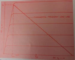
Fig. 8. Ideal Class-B load linefor microwave transistors.
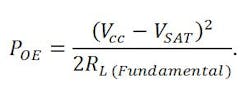
The ideal Class-B collector load line is shown in Fig. 8, where VSAT is the rf saturation voltage—higher than the dc value. The relation between power output, VSAT, and supply voltage is given by the equation:
From this equation, the effects of VSAT vs Vcc are shown in Fig. 9. It can be seen that VSAT has a significant effect on the maximum power output capability of a transistor. Thus, this is an important parameter from the standpoint of both circuit design and device design and must be taken into account when calculating the required load line to achieve a given power output.
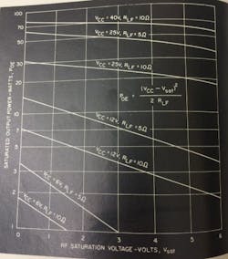
Fig. 9. How saturated output power varies with rf saturation voltage with typical microwave transistors.
Read the next part in this series here.
