REVEALED: Source Of Low-Frequency 1/f Noise
This file type includes high resolution graphics and schematics when applicable.
Although 1/f (or “pink” or “flicker”) noise was first discovered in vacuum tubes in 1925, it has been found everywhere from human heart rates to electrical currents in materials and devices. In most material systems, however, its origin has remained a mystery. In electronics in particular, the question was whether 1/f noise was generated on the surface of conductors or inside them. At the University of California, Riverside Bourns College of Engineering, a professor and a team of researchers claim to have solved the 1/f noise problem.
This noise is actually a signal or process—one with a power spectral density that is inversely proportional to the frequency. It is a key factor in electronics, impacting electronic device size and more. In a radar or communication device like a smartphone, for example, the signal’s phase noise is largely determined by the 1/f noise level in the transistors used.
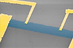
The team of researchers hailed from UC Riverside, Rensselaer Polytechnic Institute (RPI), and the Ioffe Physical-Technical Institute of the Russian Academy of Sciences. The group was led by Alexander A. Balandin, Professor of ElectricalEngineering at UC Riverside. The researchers were able toanswer questions on 1/f noise origin using a set of multi-layered graphene samples with thickness that continuously varied from around 15 atomic planes to a single layer of graphene (see figure).

Pictured is a microscopy image of the graphene device used in the 1/f experiments at the University of California, Riverside. (Image courtesy of Prof. A.A. Balandin, UC Riverside.)
According to Balandin, previous studies could not test metal films to thicknesses below about 8 nm. Graphene is 0.35 nm thick. In addition, it can be increased gradually—one atomic plane at a time. He emphasized that this study was essential for the proposed applications of graphene in analog circuits, communications, and sensors.
In addition to Balandin, who also serves as the Founding Chair of the Materials Science and Engineering Program at UC Riverside, the team of researchers included Guanxiong Liu, Sergey Rumyantsev, and Michael S. Shur, among others (see photo). The results of the research have been published in the journal Applied Physics Letters under the title: “Origin of 1/f Noise in Graphene Multilayers: Surface vs. Volume.”
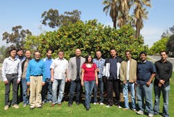
Using multi-layered graphene samples, this team of researchers has figured out what causes low-frequency electronic 1/f noise. They were led by Alexander A. Balandin, who is shown in the center (wearing the blazer). (Photo courtesy of Prof. A.A. Balandin, UC Riverside.)
The research at UC Riverside was supported, in part, by the Semiconductor Research Corp. and Defense Advanced Research Project Agency (DARPA) through the Center for Function Accelerated nanoMaterial Engineering and the National Science Foundation. The work at RPI was supported by the US NSF under the auspices of I/UCRC “CONNECTION ONE” at RPI and by the NSF EAGER program.
This file type includes high resolution graphics and schematics when applicable.
About the Author

Nancy Friedrich
RF Product Marketing Manager for Aerospace Defense, Keysight Technologies
Nancy Friedrich is RF Product Marketing Manager for Aerospace Defense at Keysight Technologies. Nancy Friedrich started a career in engineering media about two decades ago with a stint editing copy and writing news for Electronic Design. A few years later, she began writing full time as technology editor at Wireless Systems Design. In 2005, Nancy was named editor-in-chief of Microwaves & RF, a position she held (along with other positions as group content head) until 2018. Nancy then moved to a position at UBM, where she was editor-in-chief of Design News and content director for tradeshows including DesignCon, ESC, and the Smart Manufacturing shows.
