Delivering Mixed-Technology Systems Using an Agile Methodology
This file type includes high resolution graphics and schematics when applicable.
Future trends in systems point to a proliferation of mixed-technology systems. Such systems pair CMOS with non-CMOS entities in an integrated fashion. Witness the huge growth in more-than-Moore markets, such as sensors (MEMS with CMOS), for example. An integrated solution provides obvious benefits in power, cost, and area. All of these are critical for mobile as well as hyperscale back-end systems. Integrated photonics have been under research for close to a decade, and are now becoming more mainstream, increasing time-to-market pressures.
Integrated photonics components use silicon for electrical high-speed links. Their applications can include SerDes, clock data recovery (CDR), buffer drivers, and transimpedance amplifiers (TIAs). The optical components can be made from technologies such as silicon-germanium (SiGe) and indium-phosphide (InP). Unlike previous transceivers, the integrated photonics components are built in high-volume manufacturing plants and assembled just like CMOS components. Integrated photonic components enable high-density channel count at a reduced cost, allowing systems to be more compact with lower power and higher volume than previous architectures.
Presently, the silicon components are validated individually. These components are not tested together with other components until they all are assembled into the industry standard module form factor. The solution presented here is to create subsystems, which can be independently validated. This solution allows the main critical functions to be accessed for debugging before module-level integration.
Subsystem Design
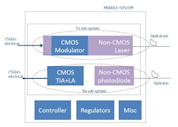
Integrated photonics is a mixed-technology system. A block diagram of the system with the transmitter (Tx) and receiver (Rx) subsystems is shown in Fig. 1. The design of the subsystem was very challenging because the data path runs at 25Gbps. Every printed-circuit-board (PCB) trace was laid out carefully and terminated with the correct impedance. A 3D EM simulator was used to simulate the entire path of the subsystem, starting from the RF connectors all the way to the optical die. A behavioral model of the optical die was created and co-simulated along with the PCB traces to ensure compliance with the industry specifications.
Subsystem Validation
In older single channel transceivers, each component was validated on an evaluation board supplied by the component manufacturer. The receiver TIA and laser driver may have been tested by themselves, but nothing occurs afterwards until all of the components are integrated at the module-level. The components are placed in close proximity to each other, which makes access to the RF paths difficult—if not impossible—at the module level. Simulations become the tool used for early predictors of system performance. However, there is no data to prove the simulations will match the final product, especially for non-silicon portions. If the simulations weren’t accurate enough, then development time is wasted and additional module-level PCB spins may be required. This is when a subsystem validation methodology can provide many benefits.
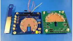
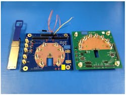
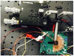
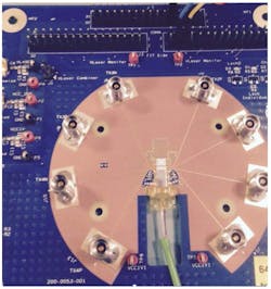
In the example under discussion, a transmit subsystem would consist of an evaluation board with the driver/CDR (silicon), laser (non-silicon), and RF inputs. Similarly, the receive subsystem consists of an evaluation board with the CDR/TIA (silicon) and receiver (non- silicon). An example of a Tx subsystem, Rx subsystem, and a form factor module is shown in Fig. 2(a).
Subsystem RF Testing
The goal of subsystem testing is to ensure that the interaction of the components in the subsystem can provide the required performance. Thus, when the subsystem is integrated into the module, the module will meet its specifications. Subsystem testing can include many of the same tests performed at the module level.
Since mature products with data rates of 10 and even 15 Gbps are already on the market, most new development is focused on higher rates such as 25 Gbps. At these RF data rates, it is imperative to maintain signal integrity through the entire test setup. High-quality electrical cables will still suffer from significant loss and signal degradation within a meter or so. In addition, subsystem evaluation boards must be designed at a high standard, as the signal quality of high-speed traces on a PCB degrade much quicker than when using RF cables. An advantage of subsystem testing is due to the subsystem in question being designed very close to the actual module implementation, with short PCB traces between the critical components.
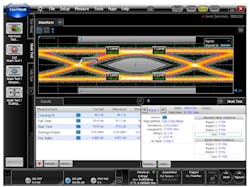
TX RF Testing. For this example, a module is developed for the PSM4 standard, which draws heavily from IEEE 802.3. As previously mentioned, the key tests are the RF output quality (eye diagram) and bandwidth tests. Rather than observing the output signal as a single waveform, sampling oscilloscopes overlay the carefully timed samples of the waveforms on top of each other [Fig. 2(b)]. Thus, all combinations of the binary data stream are seen at once.
This file type includes high resolution graphics and schematics when applicable.
Benefits of Subsystem Design, RF Testing, and Validation
This file type includes high resolution graphics and schematics when applicable.
This form of subsystem integration allows the Tx and Rx chains to be independently validated. With better access to the components for debugging purposes, it’s obvious this methodology provides the benefit of accessing all of the features from the subsystem boards that are not accessible from the module (Figs. 3 and 4).
The benefits of subsystem validation are demonstrated by listing three real-world examples below.
Quality improvement. One particular example included the discovery of I2C communication failure on the transmit driver. By using the subsystem validation method, the problem was discovered during the initial turn-on of the Tx subsystem board before all of the components were integrated into a module. Time, resources, and money were saved by using this method.
Since the subsystem evaluation board only contained the Tx parts, it was easily discovered to be a transmitter problem and the faulty component was quickly identified. If all components had been immediately built into the module, identifying the component causing the problem would have been much more difficult since any component on the I2C bus can cause the communication to fail.
Due to the I2C failure, the high-speed functionality of the Tx could not be turned on. Although this typically would have stopped all testing by means of the subsystem evaluation board, an overly pre-emphasized signal was sent to compensate for the disabled high-speed functionality. A subsystem board allowed access to internal signals that would not have been accessible in a small form factor module. Useful high-speed information was gained from what would otherwise have been a component only useful for verifying low-speed functions.
Timely Feedback to Design. The advantage of the quick feedback to design was made clear in a recent evaluation. By using the subsystem board, the bandwidth of the device was determined by measuring the S21 of the subsystem. After making this measurement, it was discovered that the low-frequency response did not match the current simulations. Because of this measurement, the simulations were updated and improvements were made.
In this particular case, the module-level PCB was not ready yet. If the subsystem validation had not been used, this issue would not have been discovered until the module-level PCB was available. Even if the module-level PCB was available, this measurement isn’t always possible on the module-level because it must be measured before the CDR, SerDes, or other components that reshape the eye and affect the bandwidth.
Quicker Iterations. The use of subsystems also enables modules and components to be developed in parallel with ease. Components that are less mature and require more design iterations can be developed and tested independently of the progress of the other components. Continuing with the I2C example, the use of the subsystem boards allowed testing and development of the RX subsystem while the Tx I2C issue was being debugged. With a module-level approach, a module-level PCB would be needed for debugging. This is much more difficult since the module PCB does not provide easy access to the components.
By removing the needs of module-level requirements, such as mechanical form factor and EMI/RF, quicker iteration of critical components is achieved. This is in accordance with lean innovation and agile methodology.
Conclusion
The design of a mixed-technology system was presented. By breaking down a system into its sub- systems and validating them separately, it is possible to get quick feedback for system improvement. With this method, development cycle time is decreased. Simulations are more accurate and effective since they are backed by real data. In addition, debugging becomes both quicker and easier. All of these improvements result in higher quality modules brought to market in less time.
As shown with real data, subsystem validation allowed the early validation of key mixed-technology systems leading to early detection of bugs/integration issues. While an optical system has been chosen, this methodology and thought process can be extended to other systems, such as consumer MEMS with wireless or other systems pairing silicon with non-silicon technologies.
This file type includes high resolution graphics and schematics when applicable.
