Benefit From High-Dk Microwave Circuit Materials
Circuit materials for microwave printed-circuit-board (PCB) applications have appreciably evolved over the past few decades. Circuit designers can now choose from a wide variety of microwave circuit materials with many different dielectric constant (Dk) values. Historically, circuit materials with high Dk values have only been used in niche applications, but that is changing. High-Dk microwave circuit materials have been used for large-volume power-amplifier applications, and these materials are also drawing interest from antenna designers. High-Dk circuit materials can offer many benefits that designers often overlook.
Just what Dk value is considered high? For microwave applications, circuit materials are commonly available with Dk values from as low as about 2 to as high as just over 10, as typically measured at 10 GHz and through the z-axis of the circuit material. Classification of circuit materials considered as “high-Dk” materials can be somewhat objective, but it typically applies to a circuit material with a Dk value of 6 or higher.
Related Articles
• Materials Support High-Speed Circuits
• Corralling Materials For Microwave Circuits
• Absorbers Highlight Material Showcase
Most circuit designers understand that by switching to a PCB material with higher Dk value, it is possible to miniaturize the dimensions of a microwave circuit for a given frequency. The size of a circuit for a particular wavelength/frequency decreases as the Dk value of the PCB material increases. Circuit materials with high Dk values can affect electromagnetic (EM) wave properties by operating with smaller circuits and shorter wavelengths and by slowing the phase velocities of the EM waves. Electric fields are also more condensed on higher-Dk circuit materials.
These simple attributes of high-Dk materials can bring numerous benefits to microwave circuits, including smaller sizes for those circuits, improved coupling, reduction in higher-order modes, reduced radiation loss, lower impedances for reasonably sized circuits, and slow-wave enhancements. They can also bring drawbacks, including increased problems with dispersion and limited high-impedance values.
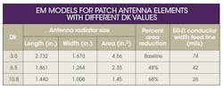
The capability to reduce the size of a circuit for a particular wavelength and frequency by using circuit materials with high-Dk values can be appealing to designers for a variety of applications. Many microwave passive components and structures are designed with physical sizes related to a fraction of the wavelength for the operating frequency, such as one-quarter wavelength or one-half wavelength. For example, many antenna designs using microwave PCB technology are patch antennas or arrays of patch antenna elements. Radiating elements for microstrip patch antennas have a length of about one-half wavelength at the frequency of interest. To explore the effects of different PCB Dk values, simple computer models were developed for a patch antenna radiating element at a center frequency of 2.5 GHz. Models were run for 30-mil-thick (0.762-mm-thick) circuit materials with Dk values of 3.0, 6.5, and 10.8, using version 13.54 of the Sonnet Professional EM simulation software from Sonnet Software. Results of the simulations appear in the table.
The simulations show the size reductions for the patch antenna element with increasing Dk value, along with a narrowing of the 50-Ω feed line with increasing circuit material Dk value. The feed line will suffer higher insertion loss with higher Dk value, which may be a concern for some applications. It can be resolved by using a coaxial cable (rather than the PCB) as the feed line to the patch antenna element. Another way around high feed line loss is to use a hybrid multilayer PCB configuration, with different circuit material Dk values for different segments of the circuit.
The Economical Approach
In some cases, a hybrid multilayer PCB configuration may help to shave costs. For example, when only a few layers of a multilayer circuit construction are critical to microwave performance, lower-cost materials such as FR-4 may form some of the layers along with the microwave materials needed for the higher-performance circuit layers. Hybrid multilayer PCB constructions may also incorporate different circuit layers to help adjust the overall coefficient of thermal expansion (CTE) of the assembly to improve the thermal reliability.
Polytetrafluoroethylene (PTFE) circuit materials offer excellent microwave performance, but suffer from high CTE properties. These materials can benefit when combined with circuit materials having lower CTE values, allowing the overall CTE behavior of the multilayer circuit assembly to be adjusted to yield a circuit that is thermally robust and reliable.
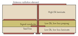
This hybrid PCB material approach might also serve to miniaturize the patch antenna while also achieving low loss with its feed lines. Figure 1 shows a cross-sectional view of a hybrid multilayer PCB that could be used to fabricate a miniature patch antenna radiating element with low feed line insertion loss. Admittedly, this is a crude illustration of this example. It merely serves to show that low-loss, low-Dk circuit material is used for the standard stripline transmission line serving as the antenna element feed line. The low Dk material allows a wider conductor for the feed line, with lower insertion loss.
Of course, there are always tradeoffs with any design approach. A hybrid circuit construction can be more expensive than a homogenous PCB in some cases (and less expensive in others) with regard to fabrication costs. For example, if a ceramic-filled PTFE material is used as the high-Dk layer and the rest of the circuit construction is low-Dk, low-loss hydrocarbon-based microwave materials, the combination can result in some fabrication cost issues. The materials are compatible, but to ensure good plated-through-hole (PTH) reliability, viaholes must be specially treated for this combination of materials. It does not add a significant cost penalty, and the desired performance results in this case can be achieved with a homogeneous material construction.
Based on commercial materials, RO4000™ circuit materials from Rogers Corp. include RO4350B™ laminate and RO4450F™ prepreg materials that could be used for the stripline feed line, while RO4360G2™ laminate can serve as the high Dk material. All of these materials have the same base substrate system, are very compatible, and use the same circuit processing approaches, so that they usually do not incur added fabrication costs. The RO4360G2 material has a Dk of 6.4; the RO4350B laminate and RO4450F prepreg have Dk values of 3.66 and 3.52, respectively.
For a further reduction in antenna element area, a circuit material with higher Dk value can be used, such as RO3210 material with a Dk of 10.8. It is a ceramic-filled PTFE material and will require different PTH preparation than the RO4000 materials. However, a simple plasma process can be used to avoid higher fabrication costs.
In addition to antennas, many high-frequency circuit applications can benefit from the use of higher Dk circuit materials. Microwave power amplifiers have traditionally used materials with a Dk range of about 3 to 4, and maintaining low insertion loss has always been one of the important reasons behind this. A few years ago, a large-volume microwave power amplifier was designed and produced with ceramic-filled PTFE material having a Dk of 6.5. Size reduction was an important initiative for this amplifier, but low insertion loss was also achieved.
Although the conductor features were reduced in width according to the Dk of 6.5, which can result in higher conductor loss, the ceramic-filled substrate material is a low-loss dielectric material which contributed to low overall insertion loss. A 25-mil-thick (0.635-mm-thick) substrate was used, and conductors were still relatively wide even at the target 50-Ω impedance. Because such a thick laminate will not be dominated by conductor loss in the manner of a thinner circuit material, it was possible to achieve good insertion-loss characteristics with this amplifier even while also achieving the size reduction.
Thermal Conductivities
Another benefit in using the higher-Dk ceramic-filled PTFE material for the power amplifier was the high thermal conductivity of the material. Thermal conductivities for PCB laminates are typically in the range 0.2 to 0.3 W/m/K, although some of the high Dk materials have thermal conductivities above 0.5 W/m/K, which is considered good. The ceramic-filled PTFE material with Dk of 6.5 used for the power amplifier had a thermal conductivity value of 0.72 W/m/K. Combined with a well-designed heat-sink configuration, this allowed the circuit laminates to effectively channel heat from the power amplifier’s active devices to the heat sink.
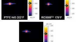
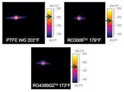
To better understand the thermal conductivity properties of microwave PCB materials, a study was conducted using several microwave laminates with a surface-mount resistor soldered to each. A DC current was used to heat the resistor and thermal imaging was performed on the different laminates. The same circuit structure was used in all cases: a 20-mil-thick microstrip circuit on 1-oz. copper, attached to a heat sink, with the only difference in each case being the substrate material. Materials with significantly different thermal conductivities were fed the same DC power levels, and Fig. 2 shows the thermal images for three of these circuits.
In all three cases, the temperatures of the resistors rose above the ambient temperature, which was about +75°F. The PTFE woven-glass (WG) circuit material at left, with thermal conductivity of 0.30 W/m/K, had the highest rise in temperature, compared to the RO3006 laminate in the middle with thermal conductivity of 0.72 W/m/K and the RO4360G2 circuit material on the right with a thermal conductivity of 0.80 W/m/K. There are many considerations when dealing with thermal management issues, and some of these considerations are covered in a prior report.1
Along with couplers and other passive components using PCB technology, there are many microwave filter applications that can benefit from high-Dk materials. Microwave filters can be reduced in size with high Dk materials but can also gain significant performance benefits. A good reference which suggests the use of high-Dk materials for filters2 shows how these materials are used to improve coupling and filter performance for mostly bandpass filters, even though lowpass and highpass filters are covered as well.
It is not unusual for a microwave circuit structure to have multiple passive components as part of its PCB design. It might include filters, couplers, impedance tuning structures, and transmission lines to connect the different circuit functions. As an example of one of these components, edge-coupled filters with half-wavelength resonators are often designed using microstrip circuit technology. Such filters can be large with lower-Dk circuit materials, but the size can be reduced through the use of a high-Dk material. The higher-Dk materials can also provide better filter performance due to the materials’ concentrated electric fields which help improve coupling between resonators.
To evaluate the impact of circuit material Dk on such filters, two microstrip edge-coupled bandpass filters were designed with the same criteria, with one implemented on circuit material having Dk value of about 3, and the other on circuit material with Dk value of approximately 10.8. Both were 25-mil-thick (0.635-mm-thick) materials with 0.5-oz. copper. The design criteria included a center frequency of 2.5 GHz, a bandwidth of 150 MHz using a Chebyshev transfer function, and passband ripple of 0.1 dB. Sonnet Software V13.54 was used to perform the EM simulations.
Filter Layouts
Figure 3 shows the layouts of the filter designs. As this figure shows, the higher Dk value results in about a 37% reduction in PCB area for the same filter. The filters were not optimized, but slightly modified to ensure that both had about the same return loss (15 dB or better) within the passband. The center frequencies and bandwidths were within a few percent of each other, so optimization was not needed for those parameters. Figure 4 shows the output of the filter performance levels according to the Sonnet software.
Both filters were nearly the same in terms of center frequency and bandwidth. A main difference is improved stopband characteristics for the filter using the material with Dk value of 3. There is some slight difference in passband insertion loss, although some of that is due to the difference in dissipation factor (Df) between the two materials. The material with Dk of 3 had a dissipation factor of 0.0016 while the material with Dk of 10.8 had a Df of 0.0027. Insertion loss was 0.61 dB for the filter on material with Dk of 3 while the insertion loss was 1.05 dB for the filter on material with Dk of 10.8. Both filters were not modeled with rough copper configurations so that simulated insertion loss would probably be higher on actual circuits.
Microwave circuits may incorporate slow-wave propagation design to reduce the size of a circuit; when combined with high Dk materials, this size reduction can be dramatic. Microwave circuits in which the size of the circuit is related to the wavelength can be reduced in size by means of slow-wave propagation since the wavelength is shortened as the wave is slowed. A reduction in the phase velocity directly relates to a decrease in wavelength, and this property can be used to shrink the size of microwave circuits.
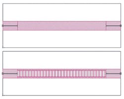
The concept of slow-wave propagation can be examining a small section of microstrip transmission line via the Sonnet Software simulator. Figure 5 shows two microstrip transmission-line circuits used for this evaluation, on 30-mil-thick substrate having a Dk value of 3. One is a normal microstrip transmission line and the other uses a ladder configuration. The ladder pattern of the conductor causes the electric and magnetic stored energies to separate in distance and that separation slows the phase velocity.
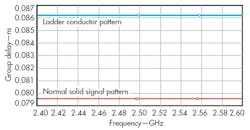
Figure 6 offers a comparison of group-delay characteristics across the passband frequency range of the filters modeled in Figs. 3 and 4. As can be seen, the group delay is slower for the microstrip transmission line using the ladder pattern for the signal conductor than for the normal microstrip transmission line.
Related Articles
• Materials Support High-Speed Circuits
• Corralling Materials For Microwave Circuits
• Absorbers Highlight Material Showcase
If the conductors for the filters in Fig. 3 were not solid copper patterns, but used the ladder effect, the geometries of these circuits could be reduced even further. However, an EM simulation model for ladder patterned conductors is extensive. Rather than perform that simulation, a general calculation was performed for the change in phase velocity/wavelength for filter size reduction.
Using the filter design of Fig. 3 as a reference, which is based on material with Dk value of 3, and comparing this to a filter on the material with Dk of 10.8 and using the ladder pattern conductors, the higher Dk value filter would be reduced in size by 41% compared to the filter using the material having a Dk value of 3. Of course, the ladder structure would affect the even- and odd-mode characteristics of the filter, so the reduction of size for this filter is reference only and the actual filter performance may be altered from what is shown in Fig. 4.
These simulation examples show just a sampling of the many uses for high Dk circuit materials in microwave applications. They can bring reductions in circuit size but, as noted, there are always tradeoffs when choosing a circuit material. When considering the use of high-Dk circuit materials to achieve a size reduction or some other benefits, a designer is advised to consult their circuit material supplier for detailed information.
References
1. John Coonrod, “Using High Frequency PCB Laminates for Improving Thermal Management Issues,” PCB West 2011 Conference & Exhibition, Santa Clara, CA, September 2011.
2. Jia-Sheng Hong and M.J. Lancaster, Microstrip Filters for RF/Microwave Applications, Wiley, New York, 2001.
Note: RO4000, RO4350B, RO4450F, RO4360G2, RO3006, and RO3210 are licensed trademarks of Rogers Corp.
