Members can download this article in PDF format.
What you’ll learn:
- How thermal analysis can be leveraged by system engineers to better understand supplier component data.
- Why determining the thermal performance of both semiconductor devices and system designs is critical.
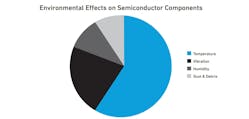
We all expect semiconductors to work reliably in the harshest environments with device failures kept to an absolute minimum. But problems inevitably arise—and from an environmental perspective, temperature is the primary reason for most semiconductor field failures (Fig. 1).
Thus, thermal design and analysis are critical to improving component reliability, with higher temperatures generally reducing component life. This can be due to a harsh operating environment without adequate system-level protection, which in turn can result from an incomplete understanding of the thermal aspects of semiconductor devices, packaging, layout, and heatsinking. In addition, it can be difficult to make thermal measurements on RF devices at the design-verification stage.
This article looks at the basic concepts of thermal behavior in semiconductors and how to practically measure and analyze temperature and thermal properties. And it covers some of the fundamentals that design engineers should understand to ensure they can create reliable systems.
Fundamentals of Thermal Properties
Let’s begin with some thermal basics. Temperature is a measurement of hot or cold—and heat is simply the product of the atoms’ energy. Thermal conduction is the transfer of internal energy by microscopic collisions of particles and movement of electrons within a material.
In any semiconductor component or system design, we must consider the thermal aspect to ensure the end-product is reliable, performs optimally, meets certification criteria, and works in all of the required environments. This means that we need to know the device temperature and how to control it.
Heat will always move from hot to cold or cooler temperatures. In addition, the amount of heat passing through something like a semiconductor or printed circuit board (PCB) depends on the thermal conductance of the material and the temperature on either side. The lower the thermal conductance of the material, the less heat will pass through for a given temperature drop.
In a semiconductor application, we always try to provide the highest thermal conductance possible for efficient heat removal from the semiconductor or heat source. The reciprocal of thermal conductance is called thermal resistance, which we wish to minimize.
In our product designs, we want to control or keep the semiconductor device as close to room temperature (about 75°F or 25°C) as possible. But as is known, this is rarely possible without a controlled environment.
Understanding Thermal Resistance and Heat Transfer
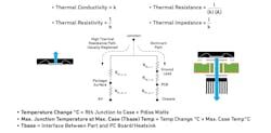
Thermal resistance is the measure of a material’s ability to resist heat flow. In general, when talking about semiconductors, we would like our semiconductor material, bonding material, PCB material, and so on, to have a very low thermal resistance (Rth), so that heat flows freely to the ambient air. Figure 2 illustrates some of the formulas associated with heat transfer and thermal measurement.
- Thermal conductivity: The ability of a given material to conduct/transfer heat.
- Thermal resistivity: The ability of a given material to resist the conduction/transfer of heat.
- Thermal resistance: Like resistivity, but it takes the shape and size of the material into account.
- Thermal impedance: Like resistance, but it doesn’t factor in the footprint size of the material and often includes interfacial resistances to provide an effective value for a layer within a stack.
The analogy of an electrical resistor network in Figure 2 illustrates the thermal resistance of a packaged semiconductor device. This represents the electrical resistor equivalent circuit, starting from the heat source (transistor junction or channel) through the two possible pathways for heat transfer.
In this electrical resistor model, the electrical resistance is defined by the potential difference (voltage) across the resistor divided by the current through that resistor. In thermal resistance, the thermal potential difference (temperature) divided by the thermal current (heat flow) through the thermal resistor defines the thermal resistance Rth.
In the first pathway, heat transfers from the transistor junction or channel through the mold compound by conduction, and then to the air surrounding the device by convection. In the second dominant pathway, which is parallel with the first, heat flows from the junction or channel of the device through the lead, through the PCB, into the chassis by conduction, and finally to the surrounding air by convection. Because most of the heat generated in the device is transported through this second pathway, it’s the primary focus for calculating the junction (or channel) temperature.
Making Thermal Measurements
In electronics, engineers use terms like junction or channel temperature, maximum temperature, heat dissipation, and power dissipation, all of which describe heat generation or the impacts thereof. When reviewing any datasheet, it’s important to understand these terms and how the thermal data lines up with your application.
The first step in understanding system thermal measurements involves looking at the semiconductor device itself. The device datasheet will provide valuable device thermal information, which can be used to determine the highest temperature or power dissipation it can handle. The datasheet reference is a good start, but in an application setting, all device interactions must also be considered.
On the device datasheet, manufacturers can use several methods of measuring and providing device thermal data. From a semiconductor perspective, manufacturers can optically measure junction or channel temperature (Tj or Tch) using one of three main methods: infrared (IR) image, thermoreflectance, and micro-Raman spectroscopy. In addition, companies will employ computer models to estimate device and system-level temperatures in a given application. Figure 3 shows the way these three methods are applied.
All three approaches in Figure 3 measure temperature without touching the surface of the semiconductor (see “Three Methods of Estimating Device Temperatures” below). IR imaging simply measures the thermal radiation coming off the surface of the semiconductor. Thermoreflectance provides its own radiation at the surface and then detects it in addition to the surface’s natural radiation (which then gets subtracted out).
Micro-Raman is a more expensive and time-consuming measurement technique. However, it’s the most accurate because it measures the temperature within the epitaxial layer with extreme resolution. In some instances, such as measuring gallium-nitride (GaN) semiconductors, this level of precision is required.
Most companies use IR imagery to make this Tj or Tch determination. It’s the easiest to use, cost-effective, and most accessible, but it provides a lower measurement value due to averaging across the surface region above the channel.
In an application, several methods are utilized to determine the temperature. One is modeling; another is IR imaging as described. Models are often used to determine temperatures in applications, but at times empirical measurements are required. Also in the mix are thermocouples or thermistors. A thermocouple measures with a voltage while a thermistor uses electrical resistance, changing its physical resistance when exposed to changes in temperature.
To perform thermal analysis of GaN devices and GaN MMICs, it’s recommended to use an integrated approach that combines device modeling, empirical measurements (including micro-Raman thermography), and finite-element-analysis (FEA) simulations.
This methodology has proven to be the most effective and accurate. With this approach, once the baseline thermal model development is completed, FEA is employed to accurately predict channel temperature and thermal resistances at the device level.
Performing System-Level Thermal Analysis
A successful system-level design relies heavily on having a good heat path from the semiconductor to the external environment. Careful consideration of the heat-flow path is needed at all levels—device, package, PCB, and final heatsink. High-power GaN devices will require fan-cooled, finned heatsinks or liquid-cooling systems for adequate cooling.
Semiconductor reliability is partly defined by estimating a device’s maximum junction or channel temperature to determine a projected lifetime. These values are gathered by measuring and modeling thermal resistance, power dissipation, and heat transfer.
In an application, the maximum junction or channel temperature is a key metric. Depending on a single method isn’t good practice—thermocouple/thermistor measurements, modeling, and IR imagery should all be employed. In a package, we should use a model to determine the maximum case temperature under the device to estimate the junction temperature based on package thermal resistance.
Another nice-to-have element in system-level thermal analysis is a bulk thermal model of the semiconductor component. Obtaining this model from a semiconductor supplier will help customers mimic the output heat flux of the component. It assists with customers’ estimates of maximum backside temperature of the product and what it will experience when operated in the customer’s system design. In addition, the bulk thermal model provides greater insight into how neighboring devices are impacted by the waste heat from the supplier’s product.
Thermal Analysis and Modeling Are Critical
Understanding and determining the thermal performance of both semiconductor devices and system designs are critical to ensuring your product functions optimally, reliably, and without problems, as well as maximizing its useful lifetime.
Thermal analysis and modeling is a complex subject, with methods such as FEA required for sophisticated design work. However, understanding the basics, as explained in this article, does help system engineers with design considerations and thermal measurements, enabling them to better understand the component data provided by suppliers.


