This file type includes high resolution graphics and schematics when applicable.
In 1965, Gordon E. Moore, Co-founder of Intel, observed that the maximum number of transistors per square inch of integrated circuit had doubled about every two years. Thereafter known as “Moore’s Law,” this phenomenon has marvelously been able to predict improvements in personal-computer (PC) processing power over the last half-century. Moore’s Law has conditioned us to expect that tomorrow’s computing devices should be smaller, less expensive, and more powerful. Yet its effect on the RF and microwave and instrumentation world might not be obvious at first glance. In fact, Moore’s Law has transformed two elements of the modern RF instrument by enabling new advancements in two areas: higher-performance intermediate-frequency (IF) and baseband circuitry [through improved CMOS technology], and advanced signal processing [through improvements in field-programmable-gate-array (FPGA) and central-processing-unit (CPU) technologies].
Advances in CMOS Technology
In traditional RF test-equipment design, signal processing was performed predominantly in the analog domain. Thus, large and complex analog systems were needed to amplify, filter, mix, and manipulate electric signals while dealing with the physical realities of nonlinearity, noise, coupling, interference, power dissipation, and so on. As evidence of this, consider the traditional swept-tuned spectrum analyzer. It used a bank of analog resolution-bandwidth (RBW) filters combined with a power detector to produce a spectrum display.
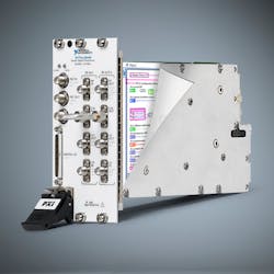
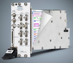
The PXIe-5644R vector signal transceiver integrates a user-programmable FPGA, RF signal generator, analyzer, and digital pattern generator/analyzer.
The alternative approach to a primarily analog instrument is to take advantage of modern analog-to-digital-converter (ADC) technology in the IF and baseband sections of the instrument. This approach requires high-bandwidth and high-dynamic-range ADCs as well as substantial signal-processing capabilities. Historically, off-the-shelf ADCs lacked both the bandwidth and dynamic range required to fully utilize the performance of the RF front end. In addition, the signal processing required to convert in-phase/quadrature (I/Q) or IF samples to spectrum data was so taxing that off-the-shelf processors would slow the performance of the instrument.
Today, advances in CMOS technology—largely driven by the wireless infrastructure market—have enabled modern RF instruments to meet or exceed the performance of traditional analog technology using off-the-shelf ADC technology. As a result, most modern RF instruments use a digital architecture that samples signals at high IFs and then converts the data to a spectrum display by means of advanced signal processing. Going forward, the design of predominantly digital instrument architectures will continue. As Analog Devices states in its 2011 Trends in Data Conversion, “The wireless communications market will remain another key driver of data converter performance, power efficiency, and calculated integration…and it’s clear that the future of high-speed converters in this market will be defined by lower power consumption combined with faster sampling rates and more usable bandwidth at higher intermediate frequencies.”
Going forward, the demand for increasingly wider bandwidths on RF signal analyzers will continue to drive the adoption of new architectures. For example, recent RF instrument designs incorporate the latest communications-infrastructure data converters and zero-IF (ZIF) modulators and demodulators. These architectures feature several advantages over traditional architectures including lower cost, less power consumption, and high selectivity. When combined with advanced calibration techniques to minimize traditional ZIF impairments, such as carrier and image suppression, these architectures often can meet or exceed the performance of traditional IF VSAs. This capability is useful in testing the latest wireless and cellular connectivity standards, such as IEEE 802.11ac. Those standards utilize up to 160-MHz signal bandwidths and require a reasonably high signal-to-noise ratio (SNR).
Greater Use of FPGAs in Instrumentation
The reasons behind Moore’s Law’s prediction of exponentially increasing PC capabilities might be obvious. Yet faster processing technology has substantial benefits for the RF instrument as well. Today, the FPGA is one processing technology that is revolutionizing the way we design RF instruments.
Having powerful and programmable FPGA-based digital signal processors (DSPs) at the center of test equipment has several advantages. First, FPGAs are parallel in nature. They can therefore perform complex mathematical calculations simultaneously without involving a host processor. EE Journal states that FPGAs have outperformed DSPs, conventional processors, and even graphics processors—both in terms of raw processing throughput on a single device and when considering the amount of power consumed (“Supercomputing Today, Tomorrow, Whenever,” November 15, 2011, eejournal.com).
Another advantage of FPGA-based test equipment is that it enables customers to easily synchronize RF signals with digital communications ports on the instruments. In applications like wireless chipset testing, for example, engineers are often testing RF performance while controlling the digital interface of the device under test. Controlling both of these elements in real time with an FPGA often leads to a dramatic improvement in test time. Using this technique to test an IEEE 802.11ac radio with a vector signal transceiver from National Instruments, for instance, Qualcomm Atheros decreased test times by more than 20X over previous PXI solutions—and up to 200X over its original solution that used traditional instruments (see figure).
Moore’s Law Beyond 2013
Intel expects computing performance advancements in accordance with Moore’s Law to continue beyond the next 10 years. In addition to fueling significant CMOS and FPGA process developments for consumer electronics, this trend is fueling advances in next-generation RF test equipment. We are likely to see additional uses for technology propelled by fast-growing consumer electronic devices, which can have a disruptive effect on the cost, size, and test throughput of next-generation RF test solutions.
About the Author
David A. Hall
Senior Product Marketing Manager for RF and Communications
David Hall is a Senior Product Marketing Manager for RF and Communications at National Instruments. His activities include building product demos, providing user feedback, and writing application notes, with particular subjects of expertise include digital signal processing and digital communications systems.


