Assess Quadrature-Demodulator Noise Figure Using Vector Signal Analysis
In a direct-conversion signal chain, it is often difficult to accurately predict the noise-figure impact due to an in-phase/quadrature (IQ) demodulator. Typically, the noise figure is measured using a noise-figure meter. Yet those meters do not operate at low enough frequencies to capture representative noise data at baseband frequencies. A calibrated noise source and a spectrum analyzer with a pre-amplified input can be used to measure the noise rise through the demodulator. But this approach is limited by the sensitivity of the spectrum-analyzer setup at low baseband frequencies. A true baseband noise assessment can be orchestrated using vector-signal-analysis techniques. For example, some basic measurement techniques can be employed with a baseband vector signal analyzer to assess the noise figure of an IQ demodulator with and without interfering signals applied.
Consider the direct-conversion signal chain depicted in Figure 1. Like many receivers, the design uses a band-selective, low-noise front end. That front end is followed by a quadrature mixing process, channel selection, and signal detection. It is similar to a real intermediate-frequency (IF) sampling receiver except the signal is split into quadrature pairs as it passes through the IQ demodulator. This approach has the inherent convenience of providing the direct output of the original IQ vectors, which were used to create the wanted modulated signal.
To recognize this feature it is helpful to understand the quadrature mixing process and the associated complex math. Consider an RF input signal given by the expression:
RF(t) = (cos(ΩLO + ΩIF)t + LSB sin(ΩLO ΩIF)t
where the time-varying envelope of the upper side band is USB while that of the lower side band is LSB. As the signal passes through the demodulator core, it gets mixed by the local-oscillator (LO) signal. That signal has its in-phase component (cosine) and the quadrature component (sine), which is realized as the LO is passed through a 90-deg. phase shifter. As the LO multiplies with the RF, both high- and low-frequency terms are generated. The high-frequency terms are rejected as the signal passes through a low-pass filter. The quantitative relation and complex frequency spectrum of the signal is shown in Figure 1.
Clearly, the in-phase and quadrature components consist of USB and LSB components. If the in-phase signal is passed through a Hilbert transform, all negative frequencies get a +90-deg. phase shift. All positive frequencies get a 90-deg. phase shift. If the result is summed with the quadrature component, the LSB signal component remains while the USB signal is rejected. In a similar fashion, an inverse Hilbert transform can be performed on the quadrature signal and then summed with the in-phase signal component. This approach allows the engineer to retrieve the USB signal component and reject the LSB signal. It is evident that quadrature accuracy determines successful rejection. Prior to the quadrature summation networks, both the wanted signal and image are overlapping. It is therefore difficult to separate the two sidebands. If a zero-IF condition (ΩIF = 0) is considered, the USB and LSB vectors are found to be readily available at the output of the Hilbert quadrature summation networks. If the original signal applied was an IQ-quadrature-modulated signal of the form:
RF(t) = I(t) cos(ΩLO)t + Q(t) sin(ΩLO)t ,
the I and Q vectors would be presented at the outputs of the quadrature summation networks. In this manner, an IQ demodulator can directly demodulate an IQ-modulated signal when using a local oscillator that is tuned to the carrier frequency.
Noise Considerations
The noise figure is a measure of the decibel degradation of a signal's signal-to-noise ratio (SNR) as it passes through a noisy device. Mathematically, it is equal to 10log (F) where F is the noise factor that is equal to the SNRINPUT/SNROUTPUT. In a frequency translation process, it is important to understand the mixing process on both the signal and noise presented by the source. Generally, the noise figure is measured on a noise-figure meter by observing the rise in noise floor above the device's linear signal gain.
Page Title
The trouble presented with the mixing process is twofold. First, it is necessary to measure the output noise at a different frequency than the source noise that is applied at the input. This task requires careful calibration of the noise receiver as well as the noise source. Secondly, the noise delivered to the IF output frequency is the result of an upper and lower sideband noise contribution, which is referred to as a double-sideband noise-figure measurement.
This aspect is more apparent when inspecting the digitized signals prior to the Hilbert networks in Figure 1. Both the upper and lower sidebands are present at the outputs of the demodulator, which complicates the measurement. Because the conversion gain of each sideband may be different, it is more difficult to predict the noise figure for a single sideband. In practice, an image-rejection scheme will be employed to eliminate any noise or interference delivered from the unwanted sideband (the image). In a swept broad-frequency-range measurement, it may be impractical to measure only the contribution from a single sideband unless the mixing process offers adequate and inherent image-rejection performance.
Vector Signal Analysis
Vector signal analysis is a technique used to assess the modulation accuracy of a modulated signal. Many vector signal analyzers (VSAs) have basic spectrum-analyzer functionality along with the ability to demodulate a signal and report a variety of information about the modulated signal. The modulated signal could employ amplitude modulation, phase modulation, or a combination of both. For its part, the VSA is designed to analyze the accuracy of the signal vectors that are used to describe the waveform.
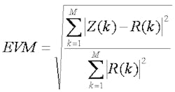
VSAs are most commonly used to measure the error vector. By measuring the magnitude and phase of each transmitted symbol, the VSA can calculate the error vector between the measured vector and the next-closest ideal constellation point. To identify the ideal constellation coordinates, the VSA must first be given the proper waveform characteristics, such as symbol rate, pulse-shaping filter specifications, and modulation format. If the error vector magnitude (EVM) is great enough that the VSA cannot correctly estimate the anticipated symbol vector, the results will be very noisy and unreliable. This is especially true in very dense modulation schemes, such as higher-order quadrature amplitude modulations (QAMs). In a time-sampled system, the EVM can be defined as:
where Z(k) is the complex received signal vector containing both in-phase (I) and quadrature (Q) components and R(k) is the ideal complex reference vector. The error vector magnitudea measure of how well a receiver performsis the ratio of the rms power of the error vector to the rms power of the reference.
Generally, a receiver will exhibit three distinct EVM limitations when compared to the received input signal power (Fig. 2). At strong signal levels, the distortion components that are falling in-band (due to nonlinearities in the receiver) will cause a strong degradation to the EVM as signal level increases. At medium signal levels, where the receiver is behaving in a linear manner and the signal is well above any notable noise contributions, the EVM has a tendency to reach an optimum level. That level is mostly determined by the quadrature accuracy of the demodulator and the precision of the test equipment.
As signal levels decrease such that noise is a major contribution, the EVM performance versus signal level will exhibit a decibel-for-decibel degradation with a decreasing signal level. At lower signal levels, where noise is the dominant limitation, the decibel EVM proves to be directly proportional to the SNR. Using this relationship, it is possible to estimate the input referred noise level of the receiver and calculate the noise figure.
Demodulator Noise-Figure Measurement
Figure 3 describes a VSA-based demodulator characterization setup. The combiner network feeding the input of the DUT allows the simultaneous application of multiple test signals. The signal path through the isolator and combiner were calibrated to get absolute power levels at the demodulator input. This provision allows for performance measurements under various blocking conditions.
For the characterization engineer, measuring the performance degradation under blocking is a serious challenge. A blocking condition is a scenario in which it is desirable to demodulate a wanted weak signal in the presence of a strong nearby interferer. Blocking tests are common requirements for a variety of cellular and point-to-point air-interface standards. The blockers may originate from another wireless terminal within the same cellular radius orpotentiallya pilot tone for cell identification from another nearby base station. A direct-conversion receiver does not have the benefit of any channel selectivity until after the signals pass through the low-noise, front-end and IQ demodulator. As a result, the front-end and IQ demodulators must support the unwanted blocker at full signal levels while maintaining sufficient sensitivity to successfully recover a faint wanted signal.
Page Title
At baseband, IQ channel-selection filters are often applied to attenuate any nearby blocking signals. They also pass the wanted signals to the IQ-digitizing analog-to-digital converters (ADCs). The noise figure of the IQ demodulator is usually of interest to system designers who want to ensure adequate cascaded sensitivityeven under blocking conditions. This measurable degradation must be managed.
Under large signal excitation, frequency-translation devices are prone to a degraded noise figure. This is partly due to the reciprocal mixing of the local oscillators' phase noise onto the unwanted blocking signal. Although the mixer cores act as multipliers in the time domain, they tend to convolve the phase characteristics of the local oscillator onto the blocker. The closer the blocker is to the wanted signal, the more likely some energy due to the oscillators' phase skirt will be present in the band of the signal of interest. Another mechanism includes blocker modulation of the flicker noise characteristics that are inherent to the mixer core. The blocking signal's RF tension can result in the square generation of DC offsets across transistor junctions in the mixer core. This signal-level-dependent DC offset can re-bias transistors and result in a change in the flicker noise characteristics. It also can affect the noise-figure performance toward 0 Hz.
VSA Noise Correction
To assess the noise figure of the demodulator and baseband VGA alone, it is necessary to compensate for the additional noise provided by the test setup. Noise analysis is more affected by the sensitivity of the analyzer than the SNR of the source. As a result, it is reasonable to correct for the analyzer noise impact alone. To measure the impact of the VSA, the demodulator was presented with a strong signal level. It could then ensure that the SNR at the output of the baseband VGA was optimum (a mean input level of approximately 50 dBm for this particular device under test ).
After the DUT, the VSA is padded with a 20-dB pad to drop the signal level somewhat into the noise floor of the VSA. This technique allows measurement of the SNR impact due to the VSA. Based on the signal gain through the DUT, the measured SNR, and the applied input level, it is possible to compute the analyzer's effective noise density. The decibel error vector magnitude (EVM) was found to be 20 dB with a 53-dBm input signal applied. This corresponds to an input voltage of 500 V rms over a modulated bandwidth of 1 MHz with a shaping filter that has an alpha factor of 0.35.
This wideband voltage is the result of a sourced signal density of 431 nV/√Hz integrated over a 1.35-MHz analysis bandwidth. The gain of the demodulator plus the baseband amplifier was measured to be 25 dB, which was followed by ~20 dB of loss due to the applied output pad. The signal densities applied to the I or Q input ports were thus ~5 dB greater than the level applied at the demodulator input, resulting in a 20-dB EVM.
Note that the EVM performance without the pad was much better. These results indicate that the pad was indeed dropping the signal level enough for the system to be dominantly limited by the sensitivity of the VSA inputs. This measurement indicated that the noise density of the VSA inputs must be ~20 dB below the signal density applied. This suggests that the VSA inputs present ~77 nV/√Hz.
Using the measured data in Figure 4 along with the calculated VSA input noise density, it is possible to compute the effective noise figure of the DUT. When sweeping the input power of the wanted signal with no blocker applied, the EVM was measured to be ~ 20 dB at a 71-dBm input level. This was measured over a 1.35-MHz analysis bandwidth. From this measurement, one can anticipate a 0-dB SNR for a 91-dBm input level, suggesting an input power density of 152.3 dBm/Hz. Into a 50-Ω impedance level, this voltage density is 5.4 nV/√Hz.
A portion of this noise is due to the VSA noise contribution. The input referred contribution due to the VSA is calculated to be 4.3 nV/√Hz. Keeping in mind that the total noise density is the vector summation of the DUT plus test equipment, one can find the DUT contribution to be 3.3 nV/√Hz. At a 50-Ω impedance level, this is a noise figure of 17.3 dB. Similar computations were made with and without blocking signals applied for zero-IF and a 5-MHz low-IF test condition.
A summary of the measured performance using the VSA in comparison to a traditional Y-factor measurement approach is provided in the Table. The Y-factor approach cannot be applied at zero-IF condition, as the test equipment used does not provide sufficient sensitivity at 0 Hz. The VSA approach proves to be a reasonable qualitative solution for assessing the demodulator noise figure at baseband. It's a useful tool for bench characterization and debug. Yet the variance of the measurement at lower signal levels may prove to be too great to be considered a quantitative solution for production characterization.
