This file type includes high resolution graphics and schematics when applicable.
It is impossible to deny the significant performance capabilities that gallium-nitride (GaN) high-electron mobility transistors (HEMTs) have bestowed upon all but the most niche technologies. In terms of power density, frequency capability, and bandwidth, there are few other technologies that compare. These factors have created a gulf between past modeling and characterization technologies and what is needed today.
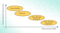
But GaN HEMTs most likely represent just the first round of next-generation high-performance technologies that will revolutionize the RF industry. To pave the way for the next round of technologies, computer-aided-design (CAD) techniques must rapidly advance (Fig. 1).
The complexity and performance of GaN HEMT devices is currently limited by two main factors: the ability to effectively design circuits that make full use of the technology’s capability, and the ability to flow enough thermal energy from GaN transistors to operate these devices at peak performance. Sophisticated modeling and characterization techniques can aid in the design process of HEMT devices, potentially mitigating the effects of these limitations.
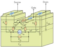
To accomplish the level of detail, efficiency, and accuracy required to perform this type of value-added simulations, the latest test and measurement and modeling techniques must be employed (Fig. 2). Power-amplifier (PA) test techniques are commonly employed to evaluate GaN transistors, as GaN technology lends itself particularly well to this application.
“Accurate active device models form the heart of basic power-amplifier design,” notes Timothy Boles, technology fellow/director of strategy for Macom. “These models need to go further than just predicting IV characteristics and output-power levels. In order to optimize overall amplifier efficiency, the models need to provide simulations that accurately reflect the active-device input and output impedances.”
Given the high-end performance of GaN HEMT technology, even minute inaccuracies in a design can significantly impact the overall performance of the final devices. Boles continues, “This enables the optimal matching topology to be presented for the amplifier input/output and—most importantly—all interstage terminals in order to achieve the lowest loss with the minimum number of transformation sections.”
GaN, as a material, is a class-III/V, compound wide-bandgap semiconductor with many incredible mechanical and electrical properties. GaN technology has been employed in applications ranging from violet laser diodes to high-frequency and high-power electronics. Thanks to GaN’s rugged mechanical properties, GaN transistors can operate in extreme environments as solar cells in satellites and in other hazardous aerospace applications. GaN also is a mechanically strong material. As a result, it can be deposited as a thin film on silicon, silicon carbide, GaN, sapphire, diamond, and even more insulating materials.
Many aspects of GaN technology are exciting for researchers, commercial companies, and military technologists alike. The challenge lies in effectively developing simulation models that are precise enough to unleash those aspects. Several techniques have been adapted from the last generation of high-performance RF substrates. In addition, several new techniques are emerging to bridge the gap.
“One high-performance technique used to characterize GaN transistors is based on the pulsed-IV characterization system,” explains Dr. Christophe Charbonniaud, deputy director and compact modeling leader for AMCAD. “The pulsed-IV method was originally developed for gallium-arsenide (GaAs) devices and has been extended to GaN devices. Principal evolutions are concerned with the increase of voltage, current swing, and commutation times when dealing with high voltages and currents.”
Using pulsed-IV characterizations demands the generation of certain measurements, which could enable the extraction of a transistor’s isodynamic equations. The trapping characteristics and thermal parameters that function as a product of the quiescent bias conditions are isodynamic parameters. If those parameters are characterized properly, they will enable the modeling of GaN transistors closer to real-world bias conditions and behavior.
For example, thermal failure based on electron trapping issues is a significant concern. It also is difficult to model using DC IV testing. As a result, pulsed-based measurements have become invaluable for accurate model development.
Beyond IV characteristics, pulsed-based S-parameter measurements have recently been used to further detail the self-heating effects and thermal dependencies within these models. The process for deriving the pulsed S-parameters and IV characteristics involves the development of a device’s early model data, which is manipulated to include the device’s scale. These parameters are then analyzed based on their accuracy toward physically measured device parameters. Fits and adjustments are performed on these parameters as a function of iterative testing.
Note that the devices commonly used in PAs have very low-impedance input/output parameters as a result of the very large device size. The parameters are therefore extrapolated to account for the increase in size. “Either of these modeling techniques needs to be validated by designing, producing, measuring, and iterating against actual device performance,” adds Boles. “Adding a thermal node to these models is more complex. It requires a set of equations that describe the basic material properties as a function of temperature and the resulting effect on the device terminal characteristics.”
Thermal limitations are a significant barrier to optimal GaN PA-device development. As a result, a significant amount of design effort is invested in ensuring desired thermal performance prior to fabricating runs on these devices. Boles states, “Thermal management and modeling are key to producing high-reliability/high-efficiency power amplifiers.”
This process reveals two areas where the detail of the data would limit the ability to effectively simulate device behavior: the quality of the measurement information on the device parameters and the model error that scales with the need to extrapolate on the fitted model data. In response to these issues, many companies have developed tools that enable a single-environment system.
Among those companies are National Instruments/AWR, Keysight, AMCAD, and Maury Microwave. Their single-environment systems promise to bridge the gap between test and measurement and model development. Aspects of these software suites aid in taking fundamental test data and creating models within a single environment. As a result, it is possible to more accurately process the evaluated device behavior. In addition, iterative testing can be repeated in a manner that far exceeds the accuracy of a human-controlled process.
This file type includes high resolution graphics and schematics when applicable.
Load/Source-Pull Considerations
This file type includes high resolution graphics and schematics when applicable.
While these measurements and model refinements aid in the design of initial devices, certain response characteristics must be confirmed in as realistic a test as possible. Equipped with realistic operational parameters, for example, a linear and nonlinear load/source-pull test can confirm the model’s ability to predict advanced behavior (such as suitability for high-powered and rapid pulsed jamming) while performing the latest modulation techniques.
Load/source-pull testing is done by adjusting the impedance and the load or source of a device while it is in active operation. Such operation can include modulation, power, frequency, and bandwidth performance that mimic the conditions in which the device would operate in the field.
There are many varieties of load-pull testing—namely harmonic, two-tone, modulation techniques; adjacent-channel power ratio (ACPR); error vector magnitude (EVR); and even time-domain testing.
The operational conditions of a load-pull test require more extreme electrical conditions that standard test equipment is designed to withstand. As a result, devices like large-signal vector network analyzers (LSVNAs) and nonlinear vector network analyzers (NVNAs) can be employed to enhance the depth of load-pull testing. Mechanically adjusted transmission lines are generally used to vary the impedance at the ports of a device under load/source-pull testing. Alternatively, these systems can be automated by machine control.
A device’s large signal input and output impedance can be derived by a real-time vector-receiver (VR) load/source-pull system. With effective calibration of the VR impedance measurement system to the device, the mismatch between the device’s input and source impedance can be eliminated from the model. This de-embedding of the device’s input-impedance behavior over a range of conditions enables an accurate power-gain description.
It also could reveal stability concerns that would be masked by less rigorous testing. In addition, a better understanding of a device’s power gain over the full range of operation provides better insight into device linearity.
Time-domain load/source-pull measurements are increasingly being used to validate model response. After all, the frequency-domain measurements won’t fully describe device operation—especially under nonlinear conditions. These measurements are often performed with an NVNA. Newer techniques can simulate the varying of the source impedance, called virtual source-pull. The simulated source-pull technique allows an automated characterization system to rapidly evaluate a device’s electrical parameters without lengthy and equipment-heavy source /load-pull testing.
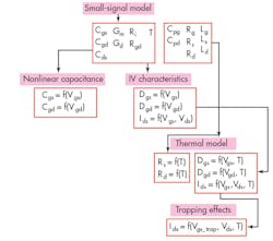
All of these techniques account for the electrical and operational behavior of a device. If the desire is to enhance a design, however, additional knowledge of the GaN device’s thermal behavior would need to be analyzed (Fig. 3). GaN devices are significantly limited by the incredible temperatures in their junctions. Methods to effectively model these extreme-temperature conditions could therefore aid in more optimal thermal designs.
“The goal is to keep the peak junction temperature as low as possible during amplifier operation,” states Boles. “This is accomplished by minimizing the thermal resistance/thermal path from the active device to the thermal heatsink—spreading out the heat-producing areas over a large area and designing heat spreading/heat-cone overlap to occur in the highest thermally conductive materials.
This is just one example of how the next generation of thermal modeling can bring tremendous value. Already, many measurement methods can estimate the temperature condition that is internal to a transistor device. There are three main ways to estimate the thermal temperature in transistor junctions: physically (with heat probes), electrically (based on the electrical transport properties of the device), and with infrared/optical methods (like micro-Raman spectroscopy).
Each of these methods has its own set of limitations and ultimately, the methods only serve as an estimation with varying degrees of error. A combination of iteratively refined modeling/simulating and device measurements is the best available technique for measuring the self-heating and channel-to-baseplate temperature gradients of GaN HEMTs.
Obviously, there is much work to be done in ensuring accurate estimations of these factors. Currently, however, this approach is the only method for deriving the characteristics associated with temperature-activated failure mechanism. It also aids the understanding of device degradation.
Charbonniaud states, “The thermal behavior of the devices can be understood in two ways: measurement and simulation. Several measurement types can be used to report the device thermal behavior including Raman, infrared (IR), and electrical testing. In our lab, we perform an electrical measurement of the temperature, which has the advantage of being easy to implement. But the drawback is that electrical-temperature testing only gives access to the mean value of the temperature.”
These tests also require the necessary laboratory equipment to implement them. As Charbonniaud notes, “To perform such measurements, a thermal chuck is needed to vary the temperature of the device and thus extract the current and charge variation as a function of the temperature.” Very detailed temperature profiles can be created of either the overall device or a device designed specifically for thermal analysis. Yet there are no viable methods to achieve the measurement-based estimation of a GaN device’s internal heat mechanisms.
In such a circumstance, the use and development of software-based techniques has enabled a functional, though non-ideal, way to more accurately predict these internal conditions. “The other way to take into account the thermal effect is by simulation,” states Charbonniaud. “Transistor meshing is first performed. Then the equations of heat are applied at each node of the mesh structure. This work is done using a 3D finite-element simulator, such as Ansys. It enables the evolution of heat flow as a function of time and its spatial distribution.”
Beyond the benefits brought by electromagnetic modeling, finite-element-modeling (FEM) and other techniques can be used to predict physical phenomena that are difficult or too costly to test. With FEM-based thermal modeling built into an interactive design-optimization simulation, there is the potential to avoid significant thermal failures in GaN devices. There also is a chance to better understand the internal mechanics of these devices.
Such techniques are giving designers a way to produce designs with greater performance more quickly than they could with traditional repetitive fabrication approaches. These simulation and CAD tools are decreasing overall cost while enabling designers to run more experiments. Eventually, these factors could help to enhance our intuitive understanding of complex device mechanics.
This file type includes high resolution graphics and schematics when applicable.


