Simulating the Stability of a Three-Stage Microwave Power Amplifier
Members can download this article in PDF format.
What you’ll learn:
- How to use software such as Microwave Office for stability analysis.
- The proper order in which to design matching networks in a multi-stage amplifier.
- The use of stability factor K and GMAX in analyzing amplifier stability.
Today’s electronic-design-automation (EDA) software gives RF engineers extremely powerful tools that can take on design tasks for all microwave circuits, beginning with the electrical schematic designs and their substrate schematic layouts, and then moving on to circuit measurements. However, designing microwave power amplifiers is a complex process that involves a specific order of tasks to achieve the final product.
This article focuses specifically on using EDA software to execute one of several available methods to simulate and analyze amplifier stability. Along the way, we’ll look at some of the steps involved so that the final product is consistent with the design goals and requirements.
The amplifier we’re looking at is a microwave integrated circuit (MIC) with bare-die components attached to an alumina substrate. There are two substrates with the first and second stages separated from the third stage by a wall that prevents cavity oscillation modes, or cavity moding. The first and second stages are based on FSX017X and FSX027X GaAs FET chips, while the third stage uses an FSX027X transistor as well. Figure 1 depicts the amplifier’s block diagram.
We used the well-known Microwave Office (MWO) software for simulation and analysis. All the figures are MWO graphs and show results from the various simulation test setups. Further down in the article, Figure 9 shows measured data of the power amplifier that was taken on a network analyzer. In this project, there was a high correlation between the simulated results and the measured data.
Dealing with Cavity Oscillations
Cavity moding can be a problem. We used a proprietary Excel program to model the internal housing cavity for potential frequencies that could create an in-band oscillation. Every internal package structure is of a given length, width, and height. These dimensions will support an electromagnetic signal that may be resonant at a frequency consistent to those dimensions.
Furthermore, not only will those dimensions resonate at a fundamental frequency, but also to higher harmonic frequencies consistent to multiples of the fundamental frequency wavelength consistent with the cavity length, width, and height. These other resonances are referred to as “harmonic moding.”
Initially, the design was plagued by an in-band TE101 modal oscillation, which was supported by the housing dimensions. The solution was to place a wall across the width of the internal cavity of the amplifier housing, thereby isolating the third stage from the first two stages. Doing so shifted the in-band cavity modal oscillation to a safe out-of-band frequency such that continued oscillation could no longer be sustained. This change occurred early in the design timeline of this project.
The first two stages are conjugately matched to each other, while the third stage is conjugately matched at the input port and power matched at the output port. A conjugate match transposes an impedance, such as R+jX to R+j0, by presenting that impedance with an interface R-jX of equal negative value. The resulting impedance match transposes 50 Ω to the real resistance only because the reactance is now zero.
A power match will interface directly to the transistor S22 parameter equivalent impedance, in both its real and reactive components, for an optimum power output with minimum network losses.
The design goals were:
- Frequency: 4 to 10 GHz
- Output power: 24 dBm
- Gain: 15 dB
- Return losses: −10 dB at input and −20 dB at output
Self-Biased Design
The system interface hardware was limited to a single positive voltage source, requiring that the design be self-biased. We placed a resistor between the three transistor source pads and ground. Self-biasing does reduce gain, but there are some advantages. First, only one positive dc power supply is required. Second, it sidesteps the turn-on vs. turn-off sequencing of the drain and gate voltages. Finally, it reduces the parts count of the dc biasing circuit.
Stages 1 and 2 constitute a single amplifier, with the stage 2 output match having been designed first. The inter-stage match between stages 1 and 2 was designed as the next step. The stage 1 input-matching network was the last network to be designed.
We designed the matching networks in that order because transistors are bidirectional and loading changes on the output side of a transistor can be seen at the input side. This process is therefore iterative, with attention going from one network to another until every network is fully designed (including layout). The dc voltage bias traces and components are therefore included in the matching networks.
Stage 3 is a single-stage amplifier with both the input and output ports designed for 50-Ω impedances. Here again, the output power match was designed first, followed by the input conjugate match.
A self-biased transistor circuit doesn’t require the positive and negative voltage sources to follow “turn-on” and “turn-off” sequences that are different from one another (turn on: negative first, then positive; turn off: positive first, then negative). A self-biased transistor has a resistor between the source terminal and ground. This creates a relatively negative gate voltage compared to the source.
A different kind of oscillation can occur between the RF microwave transistor and its corresponding dc-voltage source. A loop exists between the RF transistor and the dc source, creating a phase shift. If that phase shift becomes 360 degrees, a low-frequency oscillation (in the kilohertz range) may occur. An RC lowpass filter in the loop can back off the phase shift to between 300 and 315 degrees. The difference from 360 degrees is called the phase margin. This amplifier design was analyzed for low-frequency phase margin, but it’s not presented in this article.
K Factor
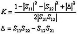
Another method of determining stability is the K factor. Stability factor K is defined by the following equation:
K is the rate of change of the drain current with respect to the reverse saturation current.
Another parameter, the maximum stable gain (GMAX), is defined as the ratio of mag(S21)/mag(S12). It’s related to K as shown by:
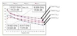
Figure 2 shows GMAX and gain for each transistor, confirming that the gain is stable over the frequency range with a safe margin. This calculation analysis was performed at up to 20 GHz using MWO software.
An amplifier is unconditionally stable when K = 1 or greater than 1, which is the goal for a single-stage amplifier. Figure 2 reveals that to achieve unconditional stability; the gain for each transistor is less than GMAX where GMAX is defined by the S parameters and K as the following (see Figure 5 for K in the case of this amplifier):
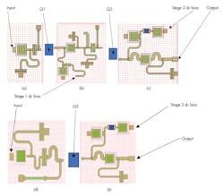
Matching networks are designed in step-by-step order, beginning with the stage 3 output match, the stage 3 input match, and then the stage 2 output match. Next come the stage 1 and stage 2 interstage matches, and finally the stage 1 input match. The matching networks are presented in Figure 3, all aligned with transistors Q1 and Q2.
The stage 1 input network is a conjugate match (Fig. 3a). The interstage network is a conjugate match between the FSX017 S22 and the FSX017 S11 (Fig. 3b). The stage 2 output and stage 3 input are a conjugate matches (Figs. 3c and 3d, respectively), and the stage 3 output network is a power match (Fig. 3e).
The dc bias voltages, traces, and components are included in the layouts of all three transistors Q1, Q2, and Q3.
The power dividers and combiners are basic four-finger, wideband Lange coupler design circuits and aren’t addressed in detail in this article. The Lange couplers provide good isolation at the input/output ports by directing the reflections to the fourth 50-Ω port.
The first two stages were designed together, matched directly to each other, and separated from stage 3, which is a single-stage design. We chose this approach because the client required a 50-Ω attenuator as a select-in-test component between stages 2 and 3.
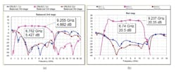
The network-analyzer graph of gain and return losses at the input/output ports is presented for stages 1 and 2 (Fig. 4a) and for stage 3 (Fig. 4b). These measurements are of the subsystem operation level of the amplifier.
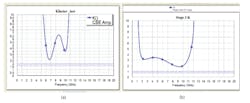
Figure 5 shows an analysis of stability K factor for this amplifier, with stages 1 and 2 shown in (a) and stage 3 shown in (b). K must be greater than 1.0 to demonstrate stability.
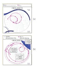
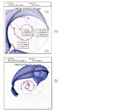
The K factor for stability is sufficient for a single-stage amplifier. However, the K factor isn’t sufficient for a multi-stage amplifier, such as the front stages 1 and 2. It’s still possible for stages 1 and 2 to oscillate with each other. The K factor will not detect internal stage-to-stage oscillations. Therefore, stability circles are required for a more in-depth analysis (Fig. 6).
If K is less than 1, or if Δ is greater than 1, circular stability regions of load/source impedances can be plotted on a Smith chart to determine where reflection S-parameters are stable or unstable. This parameter is an additional tool that can be used to work with transistors that might not be unconditionally stable.
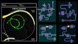
A stability circle on the Smith chart represents the boundary between values of source and load impedance that cause instability and those that do not. The perimeter of the circle is where K = 1. Sometimes the inside of the circle represents the unstable region, and at other times the outside.
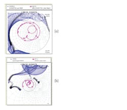
Output stability circles are the plot of load impedance. The input reflection coefficient must remain within the output stability circle for unconditional stability. Crossovers aren’t allowed at the same frequency. Figures 6b and 8a do display crossover, but further examination also shows that the crossovers occur at different frequencies.
This same analysis is performed for stages 2 and 3 (Figs. 7 and 8, respectively).
From Figures 6 through 8, it’s evident that where there are crossovers between the S-parameter reflection parameters and the stability circles (Figs. 6b and 8a), stability issues aren’t present because the crossovers occur at different frequencies.
The stability circles presented here are the result of design and analysis performed with MWO software, which, in the author’s opinion, is the microwave industry’s most accurate and easiest to learn and use. The prototype circuit was tested separately on two test fixtures (one fixture for the first two stages, and the third stage on a second fixture).
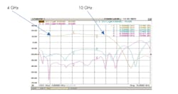
The three stages were cascaded in an additional fixture, and more network-analyzer measurements were taken. The three stages were finally tested again, all together, in the delivery housing product. The final network-analyzer measurements (Fig. 9) complied with the MWO analysis.
Conclusion
Amplifier performance (from 4 to 10 GHz) complies with the MWO simulated analysis. Other parameters complete the full spectrum of amplifier design elements (such as noise figure, IP3, IV curves, and transistor load match calculations, among others). However, this article is limited to the basic examination of the S-parameters measured on a network analyzer, and to the stability analysis of all three stages.
Acknowledgements
The author thanks Tony Nguyen and Tim Aust (the author’s mentors) for their expert knowledge of power-amplifier design, Jay Kurland for his system-perspective review, and Kathleen Farrell for reviewing this article from a professional writer’s perspective.
Kimberly Renee Alvarez is an independent consultant working as a contracting engineer. She has worked as an RF engineer at several organizations including Teradyne, L3 Technologies, Rockwell Collins, Southwest Microwave, Tampa Microwave, Raytheon, and Northrup Grumman. She holds a BSEE from West Coast University.
References
Inder J. Bahl. Fundamentals of RF and Microwave Transistor Amplifiers. Wiley. ISBN: 978-0-470-39166-2 (Hardcover)
Andrei Grebennikov, Narendra Kumar, and Binboga S. Yarman. Broadband RF and Microwave Amplifiers. CRC Press. ISBN: 13: 978-1-4665-5738-3 (Hardcover).
Stephen A. Maas. Nonlinear Microwave and RF Circuits. Artech House. ISBN: 1-58053-48 (Hardcover).
About the Author
Kimberly Renee Alvarez
Independent Consultant
Kimberly Renee Alvarez is an independent consultant working as a contracting engineer. She has worked as an RF engineer at several organizations including Teradyne, L3 Technologies, Rockwell Collins, Southwest Microwave, Tampa Microwave, Raytheon, and Northrup Grumman. She holds a BSEE from West Coast University.
