Low-Noise VCO Runs on Low Voltage
This file type includes high resolution graphics and schematics when applicable.
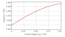
Some applications must generate their signals when only low supply voltages are available, such as in battery-powered systems. Fortunately, a quadrature voltage-controlled oscillator (QVCO) has been developed that can be fabricated with p-type metal-oxide-semiconductor (PMOS) solid-state technology. It features low phase noise and low power consumption over a moderate tuning range (5% from 2.325 to 2.440 GHz).
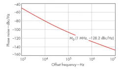
Quadrature coupling is achieved by a direct coupling technique for a reduction in power consumption, phase noise, and chip size. Suitable for a variety of wireless communications applications, the Colpitts-topology QVCO adds capacitive feedback to achieve an enhanced voltage swing over its tuning range. The prototype QVCO boasts phase noise of -128.2 dBc/Hz offset 1 MHz from a 2.34-GHz carrier while consuming only 0.535 mW power from a +0.55-VDC supply.
Quadrature signals play an important role in both wireless and wireline communication systems. They are used in a variety of different analog and digital modulation schemes, and several techniques can be employed to produce quadrature signals. For example, a VCO with a doubled frequency followed by a divide-by-two circuit can be used, as can a polyphase filter or a QVCO.1 QVCOs have been shown to be critical components in applications that require high-fidelity quadrature signals—certain communications transceivers, for example—since they can generate quadrature signals with superior phase noise and low power consumption. But designing a source capable of high-spectral-purity quadrature signals with low power consumption is still a challenge.
The simplest and most convenient way to implement a QVCO is by coupling two symmetric inductive-capacitive (LC) tank VCOs.2-4 The main drawback to this approach is the typically poor phase noise that results. In 2008, a Class-C VCO topology was proposed with a theoretical phase-noise improvement of 3.9 dB for the same current consumption as a standard differential-pair LC tank oscillator.5 Following that approach, several new Class-C VCO topologies have been proposed.5-10 However, all of these designs are based on a single differential pair configuration, similar to a traditional VCO topology.5
In quest of quadrature signals with low noise at low power levels, a new oscillator configuration was explored. In contrast to VCOs with traditional cross-coupled differential-pair LC-tank topologies, this new approach is a PMOS Colpitts QVCO. By employing a direct bulk coupling technique, this novel QVCO topology enables quadrature coupling without requiring additional transistors. In addition, it provides an enhanced voltage swing under a low supply voltage by means of a capacitive feedback technique.
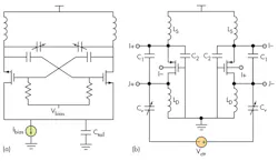
Figure 1(a) shows a cross-coupled, differential-pair, Class-C oscillator. Bias current is inserted between the NMOS source and ground and, in most cases, this is accomplished by means of a tail transistor. To filter high-frequency noise from the bias current, a large tail capacitance is employed; together with an resistive-capacitive (RC) bias network, this can prevent the transistors from working in the deep triode region.5
Figure 1(b) shows the new PMOS Colpitts VCO architecture. For a given amount of current, NMOS transistors are smaller than PMOS transistors for the same value of transconductance. However, PMOS transistors exhibit about 10-dB less 1/f noise compared with NMOS transistors. PMOS transistors also feature lower hot-carrier-induced white noise than NMOS transistors. As a result, PMOS-based VCOs can achieve better phase-noise performance than NMOS-based VCOs.11 Based on these considerations, a new VCO core was designed using a full PMOS transistor architecture.
Rather than using transistors (and their noise contributions) for quadrature signal coupling, direct bulk coupling is employed in this new QVCO to improve phase-noise performance while reducing power consumption and semiconductor chip area. To improve the oscillator’s voltage swing while operating with a low supply voltage, capacitive feedback is employed. The typical source of bias current has been replaced by an on-chip inductor, LD, leaving maximum voltage headroom for the oscillating signal and dramatically reducing the phase noise.12 This technique is especially useful in low-supply-voltage topologies.
Compared to the oscillator in Fig. 1(a), the proposed QVCO has eliminated bias voltage Vbias and the bias circuitry resistances, improving the robustness of the new oscillator’s startup functionality and reducing the thermal noise of said bias resistances. To improve QVCO startup, feedback capacitor C2 has been inserted between the PMOS source and gate. The greatest difference between the new QVCO topology of Fig. 1(b) and the traditional topology of Fig. 1(a) is that the new design employs a Colpitts architecture instead of the traditional cross-coupled differential-pair LC tank topology.
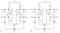
The greatest difference between the proposed QVCO and the traditional cross-coupled differential-pair LC-tank configuration of Fig. 1(a) is the use of the Colpitts architecture in the QVCO. Figure 2 presents a block diagram of the new PMOS QVCO. The four (quadrature) output ports are represented by parameters J+, J-, P+, and P-. Capacitive feedback is provided by capacitors C1 and Cv. Following the pioneering work of Hsieh and Lu,13 a simplified expression of the QVCO voltage swing for this oscillator can be represented by Eq. 1:
A ≈ (1 + C1/Cv)VDD (1)
As the simulations of the traditional VCO and the QVCO will attest, the use of capacitive feedback can greatly improve the output swing of a VCO—even when it is operating at low supply voltages.
This file type includes high resolution graphics and schematics when applicable.
A Closer Look
This file type includes high resolution graphics and schematics when applicable.
Several methods are available for achieving quadrature coupling. These include parallel-coupled QVCOs, series-coupled QVCOs, and back-gate-coupled QVCOs.14-16 For the new QVCO, quadrature coupling was accomplished by means of a bulk coupling technique, whereby an additional transistor or capacitor was not needed to provide the coupling. The use of direct bulk coupling can reduce the supply-voltage requirements.
For a MOSFET device, the threshold voltage is governed by the body effect17:
Vt = Vt0 + γ[(|2ΦF + VSB|)0.5 - (|2ΦF)|)0.5 (2)
where:
VSB = the sideband voltage;
Vt0 = the threshold voltage for VSB = 0 V;
γ = the bulk effect parameter, with a typical value between 0.3 and 0.4 V0.5; and
ΦF = a physical parameter with typical value of 0.3 V.
From Eq. 2, it is known that by applying both DC and AC bulk coupling, the effective threshold voltage can be reduced; this is desirable for achieving a low-supply-voltage, low-power oscillator design. Since forward biasing of the bulk coupling also helps to reduce flicker noise in a PMOS VCO, the use of bulk coupling leads to a coupling factor of less than unity.18 As a result, the direct bulk coupling technique can also improve the oscillator’s phase-noise performance. The design parameters for the QVCO are as follows: C1 = 429.4 fF; C2 = 664.9 fF; LS = LD = 7.1 nH; and dimensional parameters of 120/0.18 μm for M1, M2, M3, and M4.
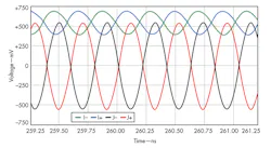
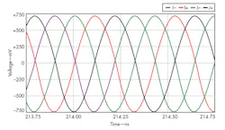
By way of comparison, circuits for the traditional VCO and the proposed PMOS Colpitts QVCO were fabricated in monolithic form using 0.18-μm RF CMOS semiconductor technology from Taiwan Semiconductor Manufacturing Company Ltd. (TSMC). The two oscillator circuits were compared in terms of output voltage swing, frequency tuning range, and phase noise. Figures 3 and 4 show the output voltage swings of the standard VCO and the PMOS QVCO cores, respectively.
As the plots reveal, the standard VCO circuit draws DC current of 486 μA when operating with a +0.55-VDC supply while the QVCO draws a higher 972 μA when running on the same +0.55-VDC supply voltage. From Fig. 3, it is known that the J- and J+ ports deliver higher output swings than the I- and I+ ports.
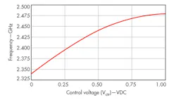
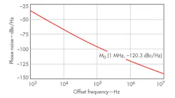
Figures 5 and 6 display the tuning ranges of the two oscillator architectures. The frequency range of the standard VCO is 2.34 to 2.48 GHz when control voltage Vctr sweeps from 0 to +1 VDC; the tuning range of the QVCO is 2.325 to 2.440 GHz when working with the same Vctr range. Figures 7 and 8 offer phase-noise performance levels for the two oscillator architectures. As these plots show, the best phase noise for the traditional VCO is -120.3 dBc/Hz offset far (1 MHz) from the carrier while the phase noise for the proposed QVCO is as low as -128.2 dBc/Hz offset 1 MHz from the carrier. In general, the performance of the new QVCO is superior to that of the traditional VCO, except for power consumption.
A figure of merit (FOM) was employed to evaluate the three performance parameters of frequency, phase noise, and power dissipation for the QVCO, as detailed in Eq. 3:
FOM = ELL(foffset) – 20log(f0/foffset) + 10log(PDC/1 mW) (3)
where:
PDC = the power dissipated by the oscillator core (in mW);
ELL(foffset) = the phase noise at the oscillator carrier frequency;
foffset = the offset frequency from the oscillator carrier; and
foffset = the center frequency.
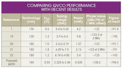
The performance of the new QVCO is summarized in the table, and compared with recent work in QVCOs. The new low-voltage design exhibits the best FOM among these reported QVCOs, with higher FOM values indicating better oscillator performance.
In summary, a new PMOS Colpitts QVCO for a +0.55-VDC supply voltage has been developed and fabricated with a commercial 0.18-μm silicon CMOS technology. By using capacitive feedback and a direct bulk coupling technique, the quadratic oscillator achieves significant improvements in terms of power consumption and phase-noise performance, making it an attractive candidate for low-power RF/microwave applications requiring low supply voltages.
On the negative side, the proposed QVCO topology requires eight inductances, which leads to a larger required chip area than some other QVCO topologies. The four tail inductances, LS, can be replaced by resistances or MOSFETs, but simulations show that this will degrade the phase-noise performance and power consumption. It will also require the use of a larger supply voltage, revealing the tradeoff of supply voltage, power consumption, phase noise, and chip area for this new QVCO design.
This file type includes high resolution graphics and schematics when applicable.
Acknowledgments
This file type includes high resolution graphics and schematics when applicable.
This work is supported by the National Natural Science Foundation of China (No. 61274020), the natural science foundation of Hunan Province (No. 14JJ7026), and the Open Fund Project of Hunan University’s Key Laboratory (No. 13K015). The authors would like to thank the anonymous reviewers for their invaluable suggestions, which helped improve the quality of this article.
Chunhua Wang, Professor and Doctoral Supervisor
Jianqun Ding, Master’s Degree Candidate
College of Information Science and Engineering, Hunan University, Changsha 410000, People’s Republic of China
References
1. F. Zao and F.F. Dai, “A 0.6-V quadrature VCO with enhanced swing and optimized capacitive coupling for phase noise reduction,” IEEE Transactions on Circuits and Systems I, Regular Papers, Vol. 59, No. 8, August 2012, pp. 1694-1705.
2. S.L. Jang, C.-C. Shih, C.-C. Liu, and M.-H. Juang, “A 0.18 μm CMOS quadrature VCO using the quadruple push-push technique,” IEEE Microwave & Wireless Components Letters, Vol. 20, No. 6, June 2010, pp. 343–345.
3. A. Rofougaran, J. Rael, M. Rofougaran, and A. Abidi, “A 900 MHz CMOS oscillator with quadrature outputs,” in IEEE ISSCC Technical Digest, February 1996, pp. 392-393.
4. S.L. Jang, S.S. Huang, and C.F. Lee, “CMOS quadrature VCO implemented with two first-harmonic injection-locked oscillators,” IEEE Microwave & Wireless Components Letters, Vol. 18, No. 10, October 2010, pp. 695-697.
5. A. Mazzanti and P. Andreani, “Class C harmonic CMOS VCOs, with a general result on phase noise,” IEEE Journal of Solid-State Circuits, Vol. 43, No. 12, December 2008, pp. 2716-2729.
6. K. Okada, Y. Nomiyama, R. Murakami, and A. Matsuzawa, “A 0.114-mW dual-conduction Class-C CMOS VCO with 0.2-V power supply,” in Symposium on VLSI Circuits Digest of Technical Papers, 2009, pp. 228-229.
7. L. Fanori and P. Andreani, “Low-phase-noise 3.4–4.5 GHz dynamic bias Class-C CMOS VCOs with a FoM of -191 dBc/Hz,” in Proceedings of the European Solid State Circuits Conference, September 2012, pp. 406-409.
8. L. Fanori, A. Liscidini, and P. Andreani, “A 6.7-to-9.2 GHz, 55-nm CMOS hybrid Class-B/Class-C cellular TX VCO,” in IEEE International Solid-State Circuits Conference, Digest of Technical Papers, February 2012, pp. 354-355.
9. M. Tohidian, A.F.-Ahmadi, M. Kamarei, and F. Ndagijimana, “High swing Class-C VCO,” in Proceedings of the European Solid-State Circuits Conference, 2011, pp. 495–498.
10. W. Deng, K. Okada, and A. Matsuzawa, “A feedback Class-C VCO with robust startup condition over PVT variations and enhanced oscillation swing,” in Proceedings of the European Solid-State Circuits Conference, 2011, pp. 499-502.
11. Z. Li and K. Ko, “A low-phase-noise and low-power multiband CMOS voltage-controlled oscillator,” IEEE Journal of Solid-State Circuits, Vol. 40, No. 6, June 2005, pp. 1296-1302.
12. N. Troedsson and H. Sjoland, “An ultra low voltage 2.4-GHz CMOS VCO,” Proceedings of the IEEE Radio and Wireless Conference, August 2002, pp. 205-208.
13. H.H. Hsieh and L.H. Lu, “A high-performance CMOS voltage-controlled oscillator for ultra-low-voltage operations,” IEEE Transactions on Microwave Theory & Techniques, Vol. 55, No. 3, March 2007, pp. 467–473.
14. A. Rofougaran, J. Rael, M. Rofougaran, and A. Abidi, “A 900 MHz CMOS oscillator with quadrature outputs,” in IEEE International Solid-State Circuits Conference (ISSCC) Technical Digest, February 1996, pp. 392-393.
15. I.S. Shen, T.C. Huang, and C.F. Jou, “A low phase noise quadrature VCO using symmetrical tail current-shaping technique,” IEEE Microwave & Wireless Components Letters, Vol. 20, No. 7, July 2010, pp. 399-401.
16. H.-R. Kim, C.-Y. Cha, S.-M. Oh, M.-S. Yang, and S.-G. Lee, “A very low-power quadrature VCO with back-gate coupling,” IEEE Journal of Solid-State Circuits, Vol. 39, No. 6, June 2004, pp. 952-955.
17. B. Razavi, Design of Analog CMOS Integrated Circuits, McGraw-Hill, New York, 2001.
18. Peng Liu, S. P. Sah, and Xinmin Yu,“Design techniques for load-independent direct bulk-coupled low power QVCO,” IEEE Transactions on Microwave Theory & Techniques, Vol. 61, No. 10, October 2013, pp. 3658-3665.
19. P. Ruippo, T.A. Lehtonen, and N.T. Tchamov, “An UMTS and GSM low phase noise inductively tuned LC VCO,” IEEE Microwaves & Wireless Components Letters, Vol. 20, No. 3, March 2010, pp. 163-165.
20. J. Chen, F. Jonsson, M. Carlsson, C. Hedenäs, and L.-R. Zheng, “A low power, startup ensured and constant amplitude Class-C VCO in 0.18-μm CMOS,” IEEE Microwave & Wireless Components Letters, Vol. 21, No. 8, August 2011, pp. 427-429.
21. A. Mazzanti and P. Andreani, “A Push-Pull Class-C CMOS VCO,” IEEE Journal of Solid-State Circuits, Vol. 48, No. 3, March 2013, pp. 724-731.
22. W. Deng, K. Okada, and A. Matsuzawa, “Class-C VCO with amplitude feedback loop for robust startup and enhanced oscillation swing,” IEEE Journal of Solid-State Circuits, Vol. 48, No. 2, February 2013, pp. 429-440.
This file type includes high resolution graphics and schematics when applicable.
About the Author

Leaders relevant to this article:


