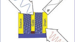
This schematic diagram shows a graphene-based subharmonic FET mixer. LO and RF signals are fed to the gate and drain terminals, respectively, while the intermediate-frequency (IF) signal is extracted from the drain terminal.
Researchers at the Chalmers University of Technology in Sweden have successfully demonstrated a subharmonic field-effect-transistor (FET) mixer at microwave frequencies based on graphene substrate material. This mixer can combine two or more electronic input signals into one or two composite output signals. The technology offers tremendous potential for use in affordable, short-distance-communications applications at terahertz (THz) frequencies.
Compared to graphene, the electron transport speed within silicon semiconductors is extremely limited. Graphene is estimated to be capable of electron transport speeds that are 100 times faster than in silicon semiconductor materials. In addition, graphene is a transparent conductor that can combine both electrical and optical signals. With its ability to switch between hole- and electron-carrier transport via field-effect mechanism, graphene also has demonstrated important potential for future RF-integrated-circuit (RFIC) applications.
The researchers at Chalmers have managed to build a graphene-FET (G-FET) subharmonic resistive mixer using only one transistor. No extra feeding circuits are required, which makes the mixer circuit more compact. Consequently, this new type of mixer requires minimal wafer area.
The G-FET also offers the potential for very high-frequency operation, thanks to the high-speed characteristics of graphene and the fact that a subharmonic mixer only requires a local-oscillator (LO) signal at one-half the frequency used by a fundamental-frequency mixer for frequency translation (see figure). This property is particularly attractive at THz frequencies, where LO power is at a premium. Moreover, the G-FET can be integrated with silicon technology. For example, it is CMOS compatible.
The coordinated development of graphene-related technology is funded by the European Commission via a 10-year, 1,000-million plan to develop a FET flagship product. The goal of this ambitious research initiative is both technological innovation and economic exploitation based on graphene and related two-dimensional electronic materials.
This major initiative follows ground-breaking experiments conducted on graphene in 2004 by European scientists Andre Geim and Konstantin Novoselov. In addition to winning them the 2010 Nobel Prize in Physics, their work sparked a scientific explosionbest illustrated by the growth of patent applications related to graphene. Huge amounts of human resources and capital are being invested into graphene research and applications in numerous countries For example, Korean chipmaker Samsung is predicting that the first graphene-based devices will appear in 2014.
The graphene flagship project already includes over 130 research groups, which represent 80 academic and industrial partners in 21 European countries. It is headed by a consortium of nine partners that have pioneered graphene research, innovation, and networking activities. Coordinated by Chalmers, the project includes the Universities of Manchester, Lancaster, and Cambridge in the UK; the Catalan Institute of Nanotechnology in Spain; the Italian National Research Council; the European Science Foundation; AMO GmbH in Germany; and the Nokia Corp.
