This article appeared in Electronic Design and has been published here with permission.
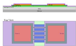
As the world battles SARS-CoV2, the virus causing the global outbreak of the disease COVID-19 or the novel coronavirus, there’s an urgent, unprecedented, and unmet demand for rapid, sensitive, specific, and low-cost diagnosis of viral antigens. Currently, the sample time for the diagnostics systems being utilized for SARS-CoV2 testing take anywhere from 5 to 15 minutes. However, biosensing field-effect-transistor (Bio-FET) devices that include advanced nanocarbon materials, which have already been proven effective in the detection of SARS, Ebola, and Rotavirus, feature sample times of mere seconds (Fig. 1).
While Bio-FET applications are an attractive next-generation platform for highly selective and ultra-sensitive virus detection, major limitations have been attached to the sensitivity of device structures and large-scale manufacturability of the semiconductor materials utilized. Since these biosensor systems rely on semiconductor materials, inefficiencies could be addressed by applying advanced nanocarbon semiconductor materials. such as nanocrystalline diamond and graphene oxide.
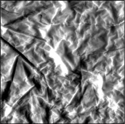
Historically, this new age nanocarbon material has been a costly, time-consuming material to fabricate. But, thanks to recent scientific breakthroughs, it can now be manufactured in batch quality at a low cost. Bio-FET devices that utilize this higher-quality nanocarbon as a device material in place of previous iterations of graphene oxide (Fig. 2) avoid limitations such as:
- Graphene flaking: Since graphene is inherently a 2D material that’s only one atomic layer thick, it’s susceptible to flaking, which completely destroys the active part of semiconductors. When this thin layer of graphene is spread across a large surface, it’s very easy for atoms to pile on top of one another or split and bond to other materials. Because there’s no stronger covalent bond than carbon to carbon, when nanocarbon materials are used, the graphene won’t bond—or flake—with anything else because its already attached to its preferential atomic bonding partner, leading to an optimized chip.
- Surface oxidation: Bio-FET devices are highly sensitive because the semiconductors are much smaller than the actual virus its detecting. Therefore, when the virus sits on top of the graphene, it can detect it easily. Oxidation happens when oxygen bonds to the graphene, instead of the virus. The nanocarbon prevents that bond.
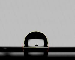
Originally developed for protective coatings of optical sensor/detector systems in Army aviation, this breakthrough nanocarbon material addresses the sensitivity, speed, cost, and manufacturing scalability associated with the presently available materials. In Bio-FET structures, a biosensor detects how electrical characteristics of systems change due to closeness or contact with analytes (Fig. 3).
A FET biosensor is comprised of a semiconductor channel, which connects the source and the drain terminals. The charged bio-molecule is attracted, immobilized, and then absorbed in the semiconductor, producing an electric field that changes the charge carrier density within the device. Nanocarbon semiconductor materials, such as graphene and nanocrystalline diamond, are particularly attractive as FET biosensor materials due to their superior electronic properties (both conductive and insulating), amphiphilicity (selectively hydrophobicor hydrophilic), biocompatibility, and chemical resistance.
While nanocarbon materials address the speed at which test results are provided, as well as manufacturing scalability, it will take more than a materials company to adequately fight the dreaded pandemic brought on by SARS-CoV2. To rapidly develop and proliferate this nanocarbon technology, and meet the global demand for faster, more affordable COVID-19 testing, partnerships must be made with labs and businesses that are already working on these biosensor applications for diagnostic systems targeting of SARS-CoV2.
Adam Khan is Founder and CEO of AKHAN Semiconductor.


