July, 1968
Copper-plated dielectric waveguide may well be considered for use in lightweight planar arrays, for waveguide components in portable microlink communications equipment, and for lightweight parabolic antenna and feed systems. Although the technique of plating dielectric substrates is not new, recent extensive research extends that work has been reported previously. Here are some of the considerations in fabrication, selection, and use of dielectric waveguides.
Selecting the dielectric
Dielectric substrates for plated-dielectric waveguide components should ideally possess the following characteristics:
- low dielectric constant (ϵ);
- low-loss tangent (tan δ);
- closed-cell structure;
- lightweight;
- low cost;
- machinable to fine surface finishes;
- operate to 212°F;
- suitable for electroless copper plating;
- commercially available in relatively large stock sizes.
Not all of these requirements are obtainable together as many are conflicting. For instance,
- lightweight vs. closed-cell structure: Below 6 lb/ft3, the substrate is open cell; 8 lb/ft3 is closed cell.
- lightweight vs. machinability to fine surface finishes. The heavier the material the finer the surface finish.
- lightweight vs. electroless copper plating. The lighter the weight, the coarser the surface finish—thus, the coarser the plated surface.
- lightweight vs. open-cell structure. These are compatible but are not suitable for high-temperature operation.
A characteristic comparison of four typical substrates investigated is shown in Fig. 1. For copper-plated dielectric waveguide applications, Polystyrene 4 lb/ft3 (commercial) appeared most suitable.
This file type includes high resolution graphics and schematics when applicapable.
Plating and preparing the raw substrate
This file type includes high resolution graphics and schematics when applicapable.
Four plating processes were investigated, all electroless—i.e., chemical reduction. These were: Enthone, Shipley, Dynachem, and MacDermid. Only two were evaluated—Dynachem and Shipley. Considerable work with the Enthone process has been performed and reported by Harry Diamond Laboratories; thus, no further work was done on this.
All plating of test pieces was done using either Dynachem or Shipley processes and in accordance with instructions pertaining to each. In the final copper plating, a 140°F Pyrophosphate bath was used with a current density of 10-15 A/ft2. A leveling agent of Unichrome Additive Agent PC-1 was added to the bath in the proportions of one quart per 100 gallons of plating solution. This additive produces a very fine surface deposit.
The required copper deposit is dependent upon conduction current, or skin depth (δ), and is determined by:
where,
λo = free space wavelength;
ρ = the conductor resistivity; and
μ = the conductor permeability.
No difficulties occurred with copper-plating adhesion to the substrate. It was concluded that good adhesion is mainly due to the mechanical locking to the pores of the machined substrate. Adhesion of molded substrates would seem to depend on interface adhesion.
A most important factor in successful plating of the raw substrate is rack design. Racking is necessary to overcome the buoyancy of the lightweight substrate. Two rack types are required. One is for the cleansing and intermediate electroless process. The other is for the final copper plating process. Both types should be heavy enough to overcome the buoyancy of the substrate and provide good clamping. In addition, the rack for the final plating process should provide good electrical contact with the substrate through relatively large contact area.
The racks should be so designed that when fitted to the substrate, forces imposed will not cause the substrate to bow, warp, or twist.
Preparing the raw substrate
Two methods for preparing the raw substrate prior to plating are machining and casting. The machining method was chosen as most convenient in this study.
To determine surface finishes obtainable, samples were prepared using three separate tools—grinding wheel, end mill, and fly cutter. The surface finishes obtained are compared in Table 1.
This file type includes high resolution graphics and schematics when applicapable.
Grinding: In the grinding operation the substrate surface was obtained with a Norton Grinding Wheel, type 32A60K5VBE. The wheel was tapered in 5°, to give a sharp cutting edge. Such a wheel may be considered to have a large number of cutting edges, thus tending to burnish as well as cut. Water was used as a coolant. Optimum conditions for grinding were obtained as follows:
- Wheel grain size 60, grain spacing 5. Finer surface finishes are not obtainable by increasing the grain size; if grain sizes from 100 to 600 were used, the wheel would “clog” between grains causing burring of the substrate.
- Optimum grinding speed 2700 rpm; feed rate 3 in./min.
End mill. For end milling, surface finish was obtained with a twelve cutting-edge end-mill cutter, which tended to burnish as well as cut. However, this process, though faster than gridning, does not produce as fine a surface finish. No cooling is required, but vacuum pickup of waste particles is necessary to keep them from impregnating the substrate.
The method of sharpening the end mill is important; i.e., the base should be sharpened before the ribs. This eliminates any burrs on the cutting edges that might score the substrate.
Fly cutter. A fly cutter has only one cutting edge, so there is no burnishing effect. Consequently a relatively coarse surface finish results. The method is quick and requires no coolant. However, the resulting surface finish proved too rough for waveguide applications.
Attenuation of plated-dielectric waveguide & joining waveguide and fitting flanges
This file type includes high resolution graphics and schematics when applicapable.
Attenuation in plated-dielectric waveguides results from copper losses (αmcu), and dielectric losses (αd). Copper losses are also a function of the presence of the dielectric.
The equations for attenuation losses are:
where,
a = wide dimension of guide;
b = narrow dimension of guide;
tanδ = loss tangent; and
λ = propagation wavelength in the dielectric.
If a material other than copper is used for plating, αtotal is found by multiplying the value for copper plating by the square root of the ratio of resistivities.
Insertion loss measurements on two test pieces of copper-plated waveguide using Eccofoam PS (4 lb), are as follows:
|
Frequency |
Length of test piece (ft) |
Theoretical attenuation (dB) |
Measured |
|
3.5 |
6 |
0.54 |
0.56 |
|
3.1 |
3 |
0.23 |
0.24 |
Joining waveguide and fitting flanges
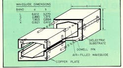
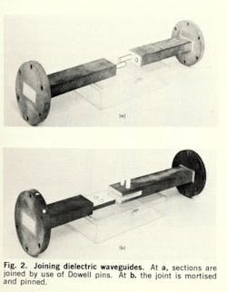
Joining methods that were developed are shown in Fig. 2. “Mortise” and “Dowell-pin” joints, similar to those used in carpentry, are shown. With these joining methods, several problems are:
- Waveguide alignment. If a misalignment of 0.03 in. exists in the narrow dimension of the waveguide, a VSWR of 1.25 results.
- Small gaps may occur between the two matting pieces. This is not considered critical because of the low dielectric constants of the substrates (ϵ = 1.08 to 1.15).
- Resistivity difference between “gluing agent” (silver epoxy) when mating pieces are jointed. If the joints are well made, and the two pieces of waveguide are well mated, this difference of resistivity is of little consequence.
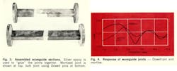
- Rigid joint and excellent electrical characteristics. The assembled joints are shown in Fig. 3. VSWR over the frequency range from 7.2 to 8.2 MHz for the assembled joints is given in Fig. 4.
Rf heating effect and the effect of solar heat
This file type includes high resolution graphics and schematics when applicapable.
To determine the theoretical temperature rise of the waveguide core, the following formula can be used:
where,
C = conductivity in BTU/hr/ft2/°F/in.;
A = cross section of the waveguide in in.2; and
l = length of the waveguide in feet.
t2 = guide temperature with power flowing
t1 = cold guide temperature
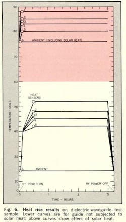
To measure heating effects along a length of copper-plated dielectric waveguide, test equipment can be set up as shown in Fig. 5.
Typical test conditions might be:
Rf input power, 320 W cw;
Frequency, 3.5 GHz;
Heat sensor, 1, 12 in. from input flange;
Heat sensors 2, 3, 4 and 5 located along the waveguide as shown;
Heat sensor 6 set to sample the ambient temperature;
Heat sensors to be calibrated against a bulb thermometer prior to test.
A typical set of measured test results are shown in Fig. 6.
Effect of solar heat
Where the waveguide is located outdoors, the effects of solar heat must also be considered. The formula for heat transfer Q is:
where,
k = constant depending on the material
A = area under the sun in ft2
∆X = average distance the heat travels from the core of the waveguide to one side.
The solar heat felt on the antenna surface depends on the sun angle and the antenna axis with respect to the sun. If the antenna is rotating, the solar heat felt will vary from maximum to minimum. How to calculate the average effect of the sun is illustrated by an example: For the antenna in our test, the maximum solar heat felt on its surface was 270 BTU/hr/ft2. If rotating, the average heat is: (1/2)(270 BTU/hr/ft2)(sin 45°) = 95.4 BTU/hr/ft2.
A black surface will absorb 0.9 (95.4) = 85.9 BTU/hr/ft2.
A medium surface will absorb 0.7 (95.4) = 66.8 BTU/hr/ft2.
A light surface will absorb 0.4 (95.4) = 38.2 BTU/hr/ft2.
Heat transfer and temperature stability
This file type includes high resolution graphics and schematics when applicapable.
Temperature stability
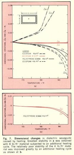
Dimensional changes in the sample waveguide cross-sections were measured when the various samples were subjected to high temperature over a prolonged period.
Each sample was measured at room temperature across the central portion of both the “a” and “b” dimensions. The samples were then subjected to a temperature of 170°F for a period of eight hours, allowed to cool, remeasured and dimensional changes noted. The procedure was repeated in steps of 5°F until a temperature of 195°F was reached. The results are shown in Fig. 7a.
The sample of Eccofoam 8lb/ft3 was subjected to an additional heating cycle, ranging from 240°F to 260°F in steps of 5°F. This material was much more stable as shown.
Each sample was then heat cycled as previously described and dimensional changes noted. The non-heat-treated sample had relatively poor dimensional stability, while the heat-treated sample exhibited good stability as shown in Fig. 7b.
Lightweight waveguide components, antennas, and feed systems
This file type includes high resolution graphics and schematics when applicapable.
Lightweight waveguide components
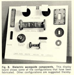
Waveguide components developed using dielectric as a substrate are shown in Fig. 8.
The rectangular waveguide components were produced by grinding of the substrate which was Polystyrene 4 lb (comm.). The circular waveguide components, of the same dielectric substrate, were produced by turning. The copper plating of the substrates was performed by using either Shipley or Dynchem process.
Lightweight antenna and feed system
A dielectric parabolic antenna and feed system is shown in Fig. 10. The antenna consists of a mirror. The antenna consists of a parabolic mirror; 18-in. in diameter with an f/d of 0.33.
The paraboloid was contoured from two solid sections of a low-loss dielectric substrate with a dielectric constant of 1.04 and loss tangent of 0.0004. Both sections of the substrate were pinned together with dielectric Dowell pins.
Due to the mirror’s size, copper plating was not possible, so the reflecting surface of the mirror was deposited by spraying with a fine silver-base lacquer, “Eccoshield ES.” The antenna feed is a dielectric conical horn integral with the parabolic mirror and fed with a circular dielectric copper-plated waveguide.
Other components
Lightweight components and integrated microwave subsystems, whose electrical performance is compatible with their conventional counterparts, can be easily and economically produced. Examples of such components are shown in Fig. 11. A complete TR subsystem, suitable for airborne operation, is shown in Fig. 12.
This new technique allows for rapid “bread-boarding” of complete subsystems. The only requirement is an inventory of straight waveguide sections plus E- and H-plane bends. With these components, the engineer can fabricate, without model shop assistance, any microwave component or subsystem and thus check a design in a relatively short time.
Recent studies point toward development of lightweight dielectric waveguide capable of carrying higher powers than are feasible to date. Such a waveguide is shown in Fig. 13. This new structure is of hexagonal cross section with rounded corners divided along its narrow dimension. Such a division is permissible because no current lines are broken by the division.
The waveguide would be constructed by casting a lightweight dielectric substrate with a density of 3.7 lb/ft3 and then copper plating. Both halves of the waveguide would be joined by dielectric Dowell pins and cemented with epoxy resin.
The purpose of the modified cross-section shape is to ease manufacture (small draw angle of about 2.5° allows for ease in withdrawing the mandrel). Rounded corners of about 0.03 in. facilitate mandrel withdrawal and allows for better adherence of copper to the dielectric substrate during plating. Mechanical inspection is also eliminated in that it is only necessary to inspect the original mandrel.
With this type of manufacture, which produces a different cross-sectional shape of waveguide, new waveguide dimensions are required as listed alongside the sketch.
This modified waveguide possesses the same guide wavelength as the conventional waveguide. Measurements of this parameter were conducted at X band, and the change in guide wavelength was 0.295%. The modified waveguide can be joined to conventional waveguide with good match. Also, the matching is independent of frequency. A prototype of the proposed modified waveguide at L band can be pressurized to 24.5 lb/in2.
