Microwave Transistor-Parameter Trade-offs in Circuit Design: Part 1
September, 1967
The rapid advance in transistor technology into the microwave-frequency region makes this article on microwave transistor trade-offs especially timely. Designers of microwave circuits using transistors should find the information presented here very helpful in their work. It will also bring other readers up to date on a subject of vital importance to the microwave industry.
Part 1 deals with basic considerations and evaluates the effect of dc parameters on microwave-circuit performance.
Part 2 will relate rf parameters to circuit performance and discuss transistor characteristics for power amplifier applications.
Part 3 will cover microwave-transistor thermal effects and VSWR considerations and will interrelate the dc-rf circuit parameters to microwave circuits. E.T.E.
This file type includes high resolution graphics and schematics when applicapable.
Part 1: Basic Considerations
Rf power transistors have recently moved rapidly into microwave applications both at sub-harmonic and direct-operating frequencies. The state-of-the-art should continue to advance, especially the maximum operating frequency, reliability, packaging and for transistors tailored to specific design applications. At present, both general purpose and tailored transistors for specific microwave applications are available. It is important, therefore, for the circuit designer to have an insight into the trade-offs involved to better understand the design problems and achievable circuit performance.
For a given transistor type and its processing, there are definite differences in high-frequency performance and interaction with the circuit. These differences can be related to the basic dc and rf parameters of the transistor. Knowing these relationships, it is then possible for the circuit designer to better understand the differences between transistors and for the equipment designer to better tailor transistor parameters to meet specific performance criteria.
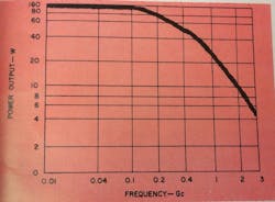
The bipolar transistor now offers reliable power outputs up to 50 W at 150 Mc and 15 to 20 W at 400 Mc. The power-frequency state-of-the-art at present is shown in Fig. 1. This is primarily for Class C, cw power output. Most microwave power generation uses Class C amplifiers at lower frequencies with multiplication, or direct Class C amplification at the planned output frequency.
Fig. 1. Power-frequency state-of-the-art for transistors operating cw Class C.
Selecting a transistor
Some basic guidelines for the circuit designer in selecting a transistor are:
- Do not introduce a transistor to a circuit that is not compatible. Understand the characteristics of the semiconductor device before designing circuits around it.
- Exercise caution in package selection. Requiring more than is needed is costly; requiring less than needed causes trouble.
- Selecting a semiconductor device on cost alone becomes a costly mistake if needed performance is sacrificed.
- Select a device which is both available and will do the proper circuit job.
- Stay within the recommended limits set by the manufacturer on its data-sheets. This requires a complete understanding of the data-sheet parameters and their interrelated use.
- Don’t overspecify the semiconductor device. Give the widest possible tolerances to save cost and improve delivery of the device from the vendor.
- Understand maximum device ratings and how to apply them in combination. Not all information on possible combinations of maximum ratings can always be included on the data sheets.
- Evaluate both the device and the circuit operation thoroughly, including all of the stress levels. Stress levels often dictate the semi-conductor device to use. How stress levels can be applied to the transistor requires a complete knowledge of its parameters and capabilities.
- Obtain assistance from the applications engineering department of the semiconductor manufacturer. It is less costly to ask a question early in the circuit design than after all of the devices have been destroyed!
Microwave transistors- how they're built
This file type includes high resolution graphics and schematics when applicapable.
To understand the characteristics of power amplifier transistors, and how parameters affect each other in combination with circuit trade-offs, the circuit designer should have a basic concept of device construction. The semiconductor die, resistor stabilization when applicable, and the packaging of the device are all very important at microwave frequencies. It is important to qualitatively relate device construction to parameters and circuit performance. Thus, one can intelligently evaluate different devices and the differences between devices of the same transistor family.
The currently most popular type of transistor construction will be described—planar epitaxial diffused junction. This type is used by all semiconductor manufacturers at present in the processing of high-frequency, power-amplifier transistors. The geometries may vary, but the concepts described here are qualitatively independent of the geometries employed. Parameters are affected by geometry, but the relationships are similar for all types.
Basic transistor construction
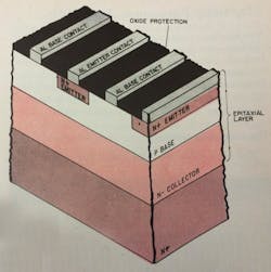
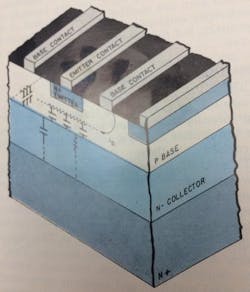
Fig. 2. Planar transistor construction. The basic elements are indicated.
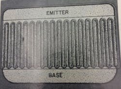
The NPN planar transistor is constructed as shown in Fig. 2. Fig. 3 is a typical top view showing interdigitated (comb structure) connections for the emitter and base areas; which is one type of connection pattern.
Fig. 3. Top view of typical planar transistor showing interdigitated comb-like structure. This is one popular connection pattern.
Transistors for higher frequencies and higher power outputs in a given physical chip area must have increased active-to-physical-area ratio. To accomplish this, a finer geometrical structure for the emitter is necessary to increase the emitter-base periphery for a given physical area. This requires smaller emitters spaced closer together. This, in turn, requires tighter mask tolerances, creating more yield problems and requiring more careful processing; thus, a more expensive device is created. Emitter geometry definition of one micron of less has been achieved in small-signal, low-power devices (one micron = 10-6 meters or 3.95 x 10⁻⁵ inches). This mask-tolerance requirement, however, cannot yet be attained in very high power, large-area transistors. The present state-of-the-art dictates emitter geometries of 3 to 5 microns in width or site side for reasonable yields.
The active area concept
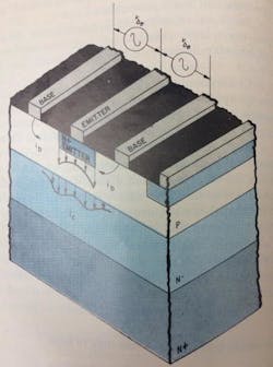
The base drive must approach the emitter-base junction from the side as visualized from the basic construction model. This base current has to go through the region under the emitter. The narrower the base width, the higher the lateral sheet resistance of the structure will be, or the higher the effective base resistance is and the more voltage drop there will be for a given base drive. Thus, the emitter-base voltage even at the edge of the emitter-base junction will not be as high as the emitter-base voltage applied across the external terminals of the device. Further, under the emitter, away from the base-contact area, less emitter-base voltage is available and the current turn-on is less as well. This is the “current pinch-off” effect.
Current pinch-off is a function of dc beta (hFE) since beta is a function of the base width. As the transistor is driven harder, the pinch-off effect becomes worse and the active area of the device (the emitter-area-carrying current) increases less rapidly than at lower current levels. What the active area looks like is roughly show in Fig. 4. Basically, this is a three-dimensional series resistance with a shunt capacitance. As frequency increases, this built-in low-pass filter allows less base-emitter junction drive. The active area decreases as the frequency increases. This, to the circuit designer, means that the transistor is shrinking in useful size or area. Unfortunately, the impedance levels are not changing as rapidly and the output capacitance is only slightly affected.
Fig. 4. Impedance representation in transistor model. The effect is a low-pass filter.
Fig. 5. Transistor current distribution for a simple transistor model.
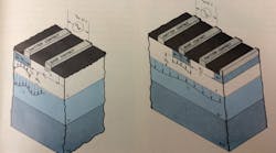
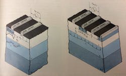
How the current distribution looks at one frequency for a simple transistor model, is shown in Fig. 5. From this sketch, it can be seen how a higher-frequency transistor (a transistor with a higher active-to-physical area ratio) would require a finer geometry. By example, Fig. 6a shows a coarse geometry compared to Fig. 6b. For the same drive at the same frequency, the current distributions would be as shown. For a given physical area, there is much more active area in the transistor of Fig. 6b because of the finer geometry. This makes the transistor more useful at this frequency. The greater active area gives more power gain for reasons that will be discussed. The transistor of Fig. 6b, however, has problems involving the safe-operating area and uniformity of operation, over the area for which something must be done to give it equivalent safe-operating performance. This also will be discussed.
Fig. 6. How finer geometry increases active area. At a is a relatively course geometry. For a given physical area, b has a more active area because of its finer geometry.
Transistor packaging
This file type includes high resolution graphics and schematics when applicapable.
Many currently-available transistors are more limited by their packaging than by the basic capability of the chip itself. This is especially so for high-frequency power devices which have relatively-low input and output impedances. The package impedances can easily be as large. Thus, a revolution is taking place in transistor packaging, especially for devices in the microwave-frequency ranges above 400 Mc.
Package inductances and resistive losses have significant effects on circuit performance—more specifically, on bandwidth, stability, power gain and phase delay. Bandwidth is important in many communications circuits, and wide bandwidth is harder to achieve with high-power transistors than for small-signal devices.
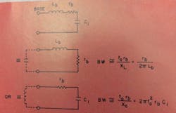
Fig. 7. Equivalent input circuit for common-emitter configuration, showing small-signal relationships between frequency, bandwidth, base resistance and input reactance.
A simple representation of a common-emitter equivalent transistor input circuit is shown in Fig. 7, demonstrating the small-signal relationships between bandwidth, base resistance and input reactance. The large-signal rb and Ci are different from the small-signal values, and an exact quantitative analysis is impossible. However, the large-signal bandwidth at the transistor input circuit will be considerably smaller than that predicted from small-signal parameter measurements. This is primarily because the effective large-signal base resistance, rb, is lower.
The emitter package inductance, Le, reduces power gain as shown in the following approximate equation.
Le also reflects an impedance into the input circuit of a common-emitter configuration (this is the most widely used configuration and the one of primary concern here). The input impedance given by small-signal analysis is (See Appendix A):
where re is the combination of transistor emitter resistance and any external emitter resistance.
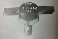
Low-inductance packaging improves both bandwidth and stability and thus ease of power matching to the transistor. A lower-inductance lower-Q circuit means less change of phase vs tuning and a wider range of stability with respect to internal feedback. An improved low-inductance package, incorporating wide-ribbon leads for the collector and base and with the emitter connected to the case for low and consistent emitter inductance, is shown in Fig. 8. This is a new concept in high-frequency packaging for transistors above 300 Mc. Still further improvement can be expected in the future.
Fig. 8. Low-inductance transistor package for 300 Mc and above. Wide ribbon leads are used for the collector and base, resulting in better stability over a wider range.
Dc parameters
If one knows a transistor’s dc parameters, he can determine what to expect of the rf parameters and of circuit performance. It is very useful to the circuit designer to understand the relationships between dc and rf parameters.
The EIA requirements for registering an rf power transistor for a 2N number are quite loose, allowing a wide latitude in parameters. All manufacturers use as wide a latitude as they can; yet, to ship good products the parameters must be controlled more closely than typical EIA registration requires. Often the parameters of distribution is tightened merely by selection of units to meet the requirements of a specific application.
Common emitter hFE and beta
DC forward current transfer ratio, hFE, is a most important control parameter for a device process. Many different rf parameters as well as circuit performance, correlate directly to hFE. It is typically measured at a low voltage and under pulse conditions so that power dissipation has no effect on it. Typically, hFE increases with junction temperature.
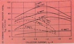
Dc beta is usually specified at both a low-current and a high-current level. Usually a minimum and maximum is specified at low-current levels; a minimum value is certainly most necessary at high-current levels. This goes back to the concept of active area and the fact that at high-current levels the current pinch-off effect occurs. At high current levels, dc beta will decrease quite rapidly when the current density has reached a high level. Therefore, low hFE devices, which have a wider base width and lower lateral sheet resistance in the base structure under the emitter of a transistor, will have more linear or constant hFE vs collector current. A high hFE device will have more radical percentage variations in hFE vs collector current. And as hFE increases, the device will reach a peak at a lower current level.
Typical relationships between hFE and collector current for different levels of hFE are shown in Fig. 9 for two different 400 Mc transistors. The curves are more linear for low hFE devices and this should significantly affect the saturation level at high frequencies and the power-output and modulation linearity. Many of the basic rf parameters also correlate directly to the hFE level of a given transistor for a given process.
Fig. 9. Relationship of hFE to Ic for two transistors at different hFE levels. The 5-W unit is designated ITT 2N3375; the 15-W transistor, ITT 3TE440.
Breakdown voltages
This file type includes high resolution graphics and schematics when applicapable.
The dc or pulse-current breakdown voltages typically specified on data sheets are:
- BVCEO(SUS) -- This is the collector-to-emitter sustaining voltage at a specified current level when the transistor is operated in avalanche with the base lead open. At high current levels, it is called LVCEO. BVCEO is the highest open-base voltage the device has in the avalanche region (the initial point). This is a guaranteed level to which the device will sustain a collector avalanche current without secondary breakdown or complete collapse of the device voltage. It is always measured in a pulse condition. Sometimes a specified quantity of energy is applied by pulsing the transistor from an inductance which has a predetermined amount of stored energy.
- BVCER(SUS) -- This is the breakdown voltage from the collector to the emitter, with a resistor connected from the base to the emitter. The measurement is made as for BVCEO(SUS). A more common designation is LVCER, or LVCES, when RBE = 0.
- BVCBO -- This is the breakdown voltage from the collector to the base and thus is the avalanche voltage of the collector-base junction. It is an important parameter because both rf parameters and circuit operation parameters correlate to this breakdown voltage. A fairly broad range of collector-base breakdown voltage is possible for a given process depending on the resistivity variation of the silicon material used.
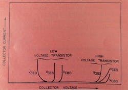
Typical breakdown-voltage curves for a low-resistivity thin expitaxial transistor and for a high-resistivity and thick-epitaxial device are shown in Fig. 10. Note that significantly different curve shapes are obtained by different transistor designs. The VSWR capabilities of the transistor are dependent on the sustaining region and these breakdown voltages.
Fig. 10. Breakdown voltage characteristics—typical transistors. Curves at left are for a low-resistivity thin epitaxial layer; at right, for a high-resistivity relatively thick epitaxial device.
- BVEBO -- This is the emitter-base breakdown voltage and is also specified at a given current level in the avalanche breakdown region. It is of secondary concern to the circuit designer where the transistor is to be operated at very high frequencies, because the stored charged rather than the external field controls the field in the emitter-base junction over most of the cycle. However, at low frequencies, this parameter is important and should be taken into consideration.
Output capacitance, common-base (Cob)
Cob is an important parameter because it affects the circuit tuning and the output-impedance level of the transistor. It also relates to some of the other dc parameters. In a common-emitter circuit, Cob is essentially the output capacitance, too. This is because the impedance levels at the base are quite low relative to the impedance level at the transistor output. However, the high-frequency value must definitely be considered and also the large-signal value (which can be as much as twice the small signal value).
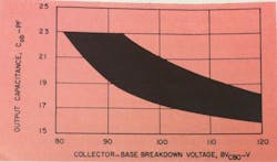
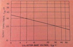
The output capacitance of a transistor represents effectively its junction capacitance in series with a resistance. If the collector resistivity is increased, the effective output capacitance is decreased as seen from the external terminals. Also, if the resistivity is increased, the collector-base breakdown voltage, BVCBO, is also increased. Junction and epitaxial-thickness variation will cause some variation in output capacitance, too. A typical distribution of COB vs. collector-base breakdown voltage is shown in Fig. 11. COB will also vary with collector voltage, which is an important consideration in large-signal operation. A typical variation in a 400-Mc transistor is shown in Fig. 12.
Fig. 11. Typical Cob-BVCBO distribution. This was obtained on a type ITT 3TE440 transistor at f ≈ 1 Mc and VCB = 28 V.
Fig. 12. Typical Cob-Vcb curve for a 400-Mc transistor, type ITT 3TE440. This variation is important in large-signal operation.
When transistors are operated in the microwave region (above 300 Mc) low output capacitance is important for good gain and high circuit impedance. Based on the “active area” concept previously discussed, it is necessary to build a finer geometric or change the material resistivity to effectively reduce the ratio of output capacitance to power capability. Changing material resistivity, however, does reduce power-output capability somewhat.
Collector-emitter saturation voltage (VCE(SAT))
VCE(SAT) is an important parameter which is always specified at dc, and which is a very misused parameter for an rf power transistor and somewhat misunderstood. Saturation voltage is specified at given collector and base currents, thus at a forced hFE (typically at the lowest guaranteed hFE, which is usually around 8 or 10).
VCE(SAT) correlates to the collector-base breakdown voltage; i.e., the resistivity of the collector epitaxial material in the transistor. Thus, a higher breakdown-voltage device has a higher saturation-voltage level at dc, and also at rf. In large-signal rf power circuits, the transistor is driven all the way from collector saturation to cutoff. Thus, the saturation level determines the extent of the voltage swing. The relationship between dc saturation and rf saturation is partly controlled by the geometry of the device because it affects the same area.
Thermal resistance (RT)
RT is an important parameter which, along with maximum-rated power dissipation, creates the actual dissipation level limits of the power devices. It is a very misunderstood rating and requires a significant understanding of high-frequency geometries and safe operating areas. In itself, thermal resistance only gives capability, provided the transistor is operated at certain collector voltages and currents as they are translated to junction temperatures and voltage fields.
Appendix
This file type includes high resolution graphics and schematics when applicapable.
Thermal resistance is not an absolute constant of the transistor because it can be different, depending on the measurement conditions.
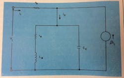
The approximate effect of Le and re can easily be shown considering the simplified T-equivalent circuit of Fig. A.
Fig. A. T-equivalent circuit with output shorted.
At high frequencies, it is convenient to represent β by the equation:
From Fig. A2,
Writing the voltage-loop equation for the input circuit, using relations (1) and (2), results in the equation:
which results in an input impedance of:
At normal frequencies of interest for normal rf power transistors,
and
Eq. 4 is then simplified to the final result:
Read the next part in this series here.
