Wideband DMOS Amplifier Competes with Bipolars
June, 1968
Double-diffused MOS (DMOS) devices offer some inherent advantages that make them strong competitors for bipolar devices in high-frequency and high-power applications. One particularly promising application of the DMOS transistor is in cable communications systems, an area currently dominated by bipolar hybrid ICs. A wideband (40-to-350-MHz) hybrid DMOS amplifier has been designed and built to demonstrate the feasibility of the device in this application.
This file type includes high resolution graphics and schematics when applicapable.
The advantages of the DMOS transistor include high input impedance, high current gain and power gain, and no thermal runway problems. Besides these intrinsic advantages, in a DMOS a very short channel length (1 μm or less) is possible without sub-micrometer lithography, and a high breakdown voltage can be obtained and tailored independently of the channel length by incorporating a lightly doped drift region between the active channel and the drain contact.
In cable communications systems, amplifiers must operate from a 24-V supply, have about 17 dB of gain and a power consumption of about 5 W, exhibit low noise over a wide bandwidth, and be very linear. The stringent distortion demands require bipolars to be overdriven (since distortion is reduced as bias increases), but overdriving causes excessive power dissipation. The potentially better distortion characteristics and the lower fabrication cost of the DMOS device may make it suitable replacement for the bipolar. Though some work has been done in this area, further investigation is needed.
The specifications chosen for the amplifier design are typical of commonly used RF amplifiers built with 2-μm-technology bipolar transistors:
- gain of 17.0 ± 0.1 dB over a bandwidth of 350 MHz,
- input and output impedances of 75 Ω with a return loss of less than -18 dB,
- 5-W maximum power dissipation, and
- second- and third-order intermodulation distortions of less than -70 and -55 dB, respectively, at signal levels of 0 dBm across the band.
Configuration choice
The choice of amplifier configuration was based on the condition that feedback be used instead of matching networks at the input and output. This condition requires higher-performance devices, but it also ensures an economical design, particularly for a multistage amplifier, which preliminary investigation showed was needed to meet the amplifier’s AC requirements.
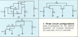
Three configurations were considered: (a) two-stage with multiple feedback, (b) cascode, and (c) cascade. Initial investigations concentrated on satisfying bandwidth and input/output requirements, with the objective of finding the configuration that best the specification while imposing the least strenuous device requirements.
The simplified AC configuration of the multiple feedback circuit shows that simultaneous shunt and series feedback resistors (RF1 and RF2) are incorporated across the stages to realize broadband and resistive input/output impedances (Fig. 1a). Input impedance is controlled by RF2, RS1, and RS2; output impedance is controlled by RF1, RS1, and RS2.
The cascade circuit (Fig. 1b) has several advantages, including minimum Miller capacitance, which results in better high-frequency performance, low noise, and the possibility of integrating two transistors into a single structure with two gates. Resistive series (RS) and shunt (RF) feedback is used to match input and output impedances. In the cascade circuit (Fig. 1c), resistive shunt feedback optimizes the input and output matches, and peaking inductors (microstrip lines) compensate the frequency response.
Performance evaluated
This file type includes high resolution graphics and schematics when applicapable.
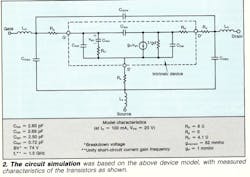
The performance of each configuration was compared using the CAD program COMPACT, which allowed each circuit to be optimized with respect to specific guidelines. A device model was selected and experimental devices were measured to come up with the required device parameters (Fig. 2).
The comparison was based on the following:
- The two devices in each amplifier would have the same dimensions, current handling capability, and drain current (at a supply voltage of 24 V). The possibility of using a smaller device for the input, with a potential noise reduction, was considered, but little advantage would have been gained in high-frequency performance.
- A device channel width, Z, of 0.4 cm was chosen in order to provide a current handling capability of 100 mA per device.
Despite its high-frequency performance, the input and output matching of the cascode circuit was poor, and the circuit began to oscillate at 160 MHz. Also, the high output impedance of the cascode stage resulted in a high output return loss. When this was combined with the high feedthrough due to the capacitance of the commongate DMOS device in the cascode configuration, CDS, the amplifier became potentially unstable. The input return loss was also high due to the low input impedance.
The multiple feedback configuration had high input and output return losses at low frequencies, due to the low input and output impedances, which were the result of the shunt feedback in the input and output. Since the DMOS devices have significantly lower transconductance than bipolar devices, they can withstand very little series feedback.
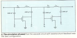
The analysis showed the cascade configuration to be the best of the three tested. With the devices used in the comparison, the cascade circuit satisfied the requirements for gain and input/output return loss up to 350 MHz.
The circuit analysis also indicated that the most important capacitance for determining the amplifier’s high-frequency performance is the Miller capacitance, CGD. In addition, CGS, CGC, and CGD are important in determining input matching, and CDS and CGD are important in determining output matching.
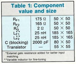
A simplified AC configuration of the circuit (Fig. 3) shows the resistive shunt feedback used to optimize the input and output matching and the peaking inductors used to compensate the frequency response. The 2000-pF blocking capacitors were employed to isolate the DC biasing circuit from the feedback network.
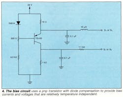
The biasing circuit, which was designed to providing biasing currents and voltages that would be relatively independent of temperature, uses a pnp transistor with diode compensation (Fig. 4). Isolation networks decouple the RF signal from the biasing network. Terminals G1 or G2 and D1 and D2 connect directly to the gates and drains of the amplifier’s transistors.
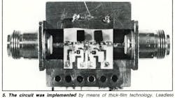
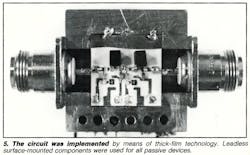
An experimental amplifier was built using devices fabricated by a DMOS process with 4-μm minimum linewidth and 2-μm alignment tolerance. The two devices chosen for the circuit had the same dimensions, current handling capacity, and drain current. The circuit was implemented by means of thick-film hybrid technology. Leadless surface-mounted components were used for all passive devices to simplify fabrication. The components and transistors were mounted onto the substrate, and the transistors were wire-bonded to the circuit (Fig. 5).
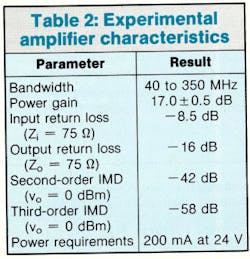
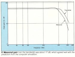
The amplifier exhibits a power gain of about 17 dB over the desired 40-to-350-MHz bandwidth, in good agreement with the results predicted by the COMPACT simulation (Fig. 6). The input and output return losses were measured at -8.5 dB and -16 dB, respectively, over the same bandwidth.
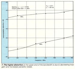
At 200 MHz, the measured second-order intermodulation distortion was -42 dB and the third-order IMD was -58 dB (Table 2). Higher distortion was measured at higher frequencies due to decreasing loop gain and increased parasitic losses (Fig. 7).
The performance of the DMOS amplifier with 4-μm-linewidth devices was compared to commercially available amplifiers using 2-μm bipolar technology. Gain, bandwidth, output return loss, third-order IMD and power dissipation were all comparable. However, the DMOS amplifier’s second-order IMD and input return loss need significant improvement. The better second-order IMD in the bipolar amplifier is the result of a balanced configuration, and the high-input return loss in the DMOS amplifier is due to untrimmed resistors used in the feedback loops.
To improve the amplifier’s performance, higher-frequency devices must be used and improvements in device and amplifier distortion need to be considered. Third-order IMD can be reduced by decreasing channel length and width, the gate oxide capacitance, and the n- epilayer doping concentration and by biasing the device at a higher drain-to-voltage. Second-order IMD can be greatly improved by using a balanced amplifier configuration. In addition, for better control of the amplifier’s performance and improved input return loss, the feedback components must be trimmed.
A monolithic version of the cascade circuit used in the DMOS amplifier is not practical because large capacitors and inductors cannot be integrated. Other circuit configurations, such as differential amplifiers, might be feasible, however, and they are being investigated.
This file type includes high resolution graphics and schematics when applicapable.
