Novel Microstrip Antenna Aims at UWB Applications
This file type includes high resolution graphics and schematics when applicable.
Use of ultrawideband (UWB) signals holds great promise for reliable wireless communications at high data rates. In 2002, the U.S. Federal Communications Commission (FCC) designated the frequency band from 3.1 to 10.6 GHz for commercial use of UWB communications technology, prompting researchers to explore different antenna designs for that frequency range.1-4 Today, researchers continue that pursuit, recently developing a compact monopole antenna with a single-slotted ground plane and stepped rectangular resonator structure. It measures just 20 × 15 mm2 and achieves VSWR of less than 2.00:1 from 2.65 to 10.00 GHz.
Successful implementation of these UWB wireless-communications systems depends on effective and compact antennas with near omnidirectional radiation patterns. Such antennas are also required for radar, medical imaging, and radio-frequency-identification (RFID) applications, in support of high data rates at low power levels.5
Printed monopole antennas have received lots of attention in recent years for their simple topologies, wide impedance bandwidths, low cost, omnidirectional radiation patterns, and relative ease of fabrication. Simple feed structures also make these antennas attractive for use in wireless-communications integrated-circuit (IC) technology. Different structures and approaches have been employed to fabricate these antennas, with varying degrees of success.6,7 The candidate antenna, designed for a broad bandwidth, is a printed planar monopole design.
Printed microstrip slot antennas have seen wide use in commercial and military wireless applications.8-10 They offer many benefits, including compact size, light weight, ease of implementation, and low cost, and can be easily integrated with microwave circuits. The most common antenna topology is a rectangular and circular patch.
Refining the Microstrip
Of course, microstrip patch antennas also suffer some disadvantages, including low gain and low impedance bandwidth. Several techniques have been applied to overcome these limitations, emphasizing large bandwidth and small size. In one, an antenna with a meandering form achieved improved gain through a genetic algorithm.11 Another design employed a Hilbert curve fractal for RFID applications.12,13 A third approach relied on high-permittivity dielectric substrate material to minimize printed antenna size.14 Unfortunately, this choice of material increases the flow of surface waves and reduces antenna gain.
A number of different UWB antennas have been realized for applications from 3.1 to 10.6 GHz, including an ring antenna,15 a spline-shaped antenna,16 triangular patch antennas,17 and square printed antennas using a defected microstrip structure (DMS) with different topologies printed on substrates.
Some researchers investigated microstrip antennas combined with defected-ground-structure (DGS) technology, which is incorporated in the ground plane or with a DMS slot etched in the radiating patch. Such antennas consist of radiating structures spaced a small fraction of a wavelength above a ground plane and directly connected using an input port through a planar feed.
These various studies on UWB antennas led to improved antenna impedance bandwidths. Efforts to etch a DGS on the ground plane or a DMS on the radiating patch were used to improve the impedance bandwidth and radiation characteristics. Numerous DMS-DGS shapes with different topologies, such as an open-loop ring slot,18 a U-shaped slot,19 and a square-ring slot20 have been investigated. Other researchers have used the tunable features of different shapes to significantly increase slot antenna bandwidth, achieving wide tuning ranges for different shapes, including H-shaped,21 L-shaped,22 and C-shaped tuning-stub configurations.23
“Steps” Toward Improvement
These different efforts to cover wide bandwidths in small antenna configurations show that improvements in size and radiation properties were obtained by cutting “stair steps” into each radiating element and using an etched slot in the partial ground plane. Because such a quasi-fractal technique does not provide a sufficiently large bandwidth, a notch was inserted in the partial ground plane with the goal of increasing the antenna bandwidth.
Antenna design and optimization were performed with the aid of circuit simulations using computer-aided-engineering (CAE) design software from AWR Corp. and Computer Simulation Technology. The simulation software allowed for analysis of antenna radiation patterns and performance, including VSWR and return loss.
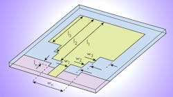
Figure 1 shows the three-dimensional (3D) layout of the designed patch antenna with its modified ground plane. The rectangular monopole antenna was printed on RO4003 circuit laminate from Rogers Corp., which has relative permittivity of 3.38 at 10 GHz in the z-direction (thickness) of the material. The circuit laminate had thickness (h) of 0.813 mm and exhibits a dielectric loss tangent of 0.00027 at 10 GHz.
To achieve wideband performance, multiple adjacent resonant frequencies should be created to obtain the desired response by driving the return loss below −10 dB within the desired frequency range. Reaching this goal required several parametric studies on the ground and patch. The fringing fields were created at resonant frequencies between the patch edges and the ground metal.
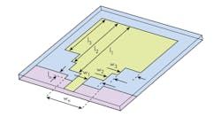
One approach to improve return loss involved widening the fringing fields by increasing total radiation; this was done by changing the ground’s dimensions to cover the area below the feed line while preserving its total width (Fig. 1a). In such a configuration, the fringing fields from the patch edges will try to reach the ground plane. This will enable the antenna to radiate around the resonant frequency. To improve the broadband impedance matching, a simple U-shaped slot was etched from the ground (Fig. 1b) with a width of 7 mm and length of 1 mm.
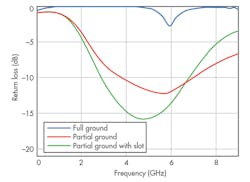
Figure 2 compares antenna return losses for different ground shapes, including an ordinary rectangular (full) ground structure that fully covers the circuit substrate and smaller structures with partial ground and partial ground with additional slot. The antenna with full ground structure had a resonance at 6 GHz and exhibited the smallest bandwidth of the antenna shapes. Return loss improved significantly by using the partial ground—return loss at resonance dropped to –12.3 dB for a bandwidth of 4.0 to 6.5 GHz. The added slot dropped the return loss to –15.7 dB for a bandwidth of 3.5 to 6.5 GHz.
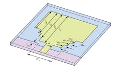
Its use in UWB applications required a significant increase in return loss around the resonant frequency, via modifications to the patch. The 6-GHz resonant frequency was obtained by designing a patch (half-wavelength resonator) with length of 13 mm and width of 15 mm. As Fig. 3 shows, the design approach involved dividing the patch into three different lengths. Each of the three lengths corresponds to a one-half-wavelength patch at a different resonant frequency, resulting in three different resonant frequencies (Table 1).
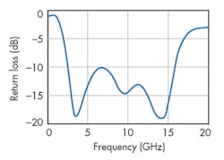
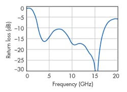
Figure 4 illustrates the return-loss response of the UWB antenna design. As can be seen from the plots, the antenna operates with return loss of better than 10 dB from 2.45 to 15.8 GHz, with total antenna bandwidth of 13.35 GHz. The width of each resonator is considered small compared to the width of a single resonator. This may explain why these obtained resonant frequencies didn’t appear obvious in these results.
A Different Approach
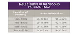
By using this same divided patch resonator concept, another antenna was simulated using four different lengths for the patch (Fig. 5). The equivalent resonant frequencies and the patch dimensions are shown in Table 2. Figure 6 offers the return loss of the proposed antenna, which behaves (Fig. 2, again) in the manner of an UWB antenna. The antenna operates from 2.65 to 16.0 GHz, a significant increase in bandwidth over the previous design configuration.
The proposed antenna was fabricated and characterized with a model HP8722D vector network analyzer from Keysight Technologies. The antenna was printed on RO4003 circuit substrate material from Rogers Corp. with a relative dielectric constant (εr) of 3.38 and thickness (h) of 0.813 mm (Fig. 7).
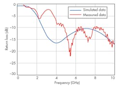
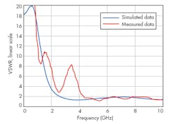
Figures 8 and 9 show the antenna’s measured return loss and VSWR, respectively. Inspecting the measurement results of Fig. 8, the experimental results demonstrate antenna operation from 4 GHz to more than 10 GHz with return loss of less than about 10 dB. Compared to simulated results, the experimental results agree closely. Some amount of frequency shift was observed between the simulated and measured results, which can be due to the imperfect full-wave simulation methods and lack of total fabrication accuracy and tolerance control.
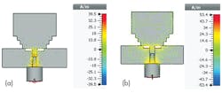
To investigate the UWB antenna’s behavior, surface-current distributions were studied at different frequency bands (Fig. 10). The current distribution was calculated at two frequency bands—the first one at 1 GHz, considered below the operating frequency range, and at 10 GHz, considered the end of the antenna’s frequency range. As can be seen, at 1 GHz, the antenna didn’t radiate and all power is reflected. But at 10 GHz, the antenna radiates effectively.
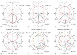
In terms of computer simulation, the directive gains of the proposed antenna in the x-z, y-z, and x-y planes were calculated at 4, 7, and 10 GHz (Fig. 11). The simulated results show the antenna to be directional in the x-z plane and omnidirectional in the other two planes, suiting the antenna for UWB applications.
Conclusion
In summary, this compact monopole patch antenna achieves a wide impedance bandwidth of 116% with 10-dB return loss at a center frequency of 6.33 GHz. It features the broadband frequency coverage from 2.66 to 10.00 GHz for WLAN applications. By adding an etched rectangular slot in the ground plane, the antenna gains improved impedance matching and radiation characteristics. An edge-cut technique was employed to reduce antenna size and enhance bandwidth, making this an attractive design candidate for many wideband wireless-communications applications.
The authors would like to acknowledge the German Research Foundation (DFG) for financial support and to thank Ms. Eng. Sonja Boutejdar for her help and Mr. Harald Dempewolf, laboratory manager of the Institute for Electronics, Signal Processing, and Communication (IIKT) at the University of Magdeburg, Germany, for support.
Ahmed Boutejdar is a professor in the Microwave Engineering Department, University of Magdeburg, Germany; Ahmed A. Ibrahim is a lecturer in the Electronic and Communication Engineering Dept., Minia University, Egypt; and Edmund P. Bunte is a professor at the Institute of Micro and Sensor Systems, University of Magdeburg.
