Capitalize on EDA When Developing MIMO, Phased-Array Antenna Systems, Part 1
Download this article in PDF format.
Phased-array antennas are becoming a popular solution in a variety of applications, with new active electronically scanned arrays (AESAs) finding their way into automotive driver assist systems, satellite communications, advanced radar, and more. The complexity and cost issues associated with developing communications systems based on phased-array antennas are being addressed through new functionalities in electronic-design-automation (EDA) software.
EDA tools support designers by providing them with the means to develop new system architectures and component specifications, as well as implement the physical design of individual components and verify performance prior to prototyping. This first part of a two-part series discusses these trends and presents recent advances in EDA tools for phased-array-based systems.
Phased-Array Primer
Electronically steered antennas are an array of individual radiating elements with phase and amplitude controlled either digitally through analog/RF components, or by using hybrid techniques to control beam direction without the need to physically move the antenna. By controlling phase and amplitude of the input signal to the individual elements, one can achieve steerable directivity of the antenna beam over both azimuth and elevation. Design considerations for an AESA radar system include the individual radiating elements (antenna design), the RF link budget of the feed network that is directly tied to component performance (e.g., insertion losses and impedance mismatch), and the array itself.
Given the complexity of the task, design groups need a system-aware approach that enables team members to explore phased-array behavior at different levels of abstraction. These development stages range from early conceptual models with little detail to highly defined array models that account for true component interactions and possible impairments. Designing the complex packaging schemes for high-frequency signaling must be addressed with circuit simulation and electromagnetic (EM) analysis tools specialized for RF and microwave electronics.
Design Management and EDA Tools
While actively steered phased-array antennas have many advantages, they are also extremely complex. Moreover, cost of production is significantly higher than conventional antenna design, especially non-recurring development costs.
As the industry shifts toward highly integrated phased-array systems, it is critical for in-house systems expertise to work closely with hardware developers to fully explore the capabilities and tradeoffs among possible architectures and integration technologies. In addition, a start-to-finish design flow made possible with EDA software has become critical in moving beyond the initial system simulation, which focuses on early architecture definition, to the development of link budgets and component specifications.
A preferred phased-array system design flow manages the start-to-finish front-end development, embedding RF/microwave circuit simulation and/or measured data of radio/signal-processing (behavioral) models within a phased-array system hierarchy. With such software, the system designer can select the optimum solution, ranging from hybrid modules through fully integrated silicon core RF integrated-circuit (RFIC) devices, to address the specific requirements of the targeted application.
Perhaps more importantly, a system-aware approach, carried throughout the entire phased-array development cycle, enables the team to continually incorporate more detail into their predictive models and observe the interactions between array components. Then they can make system adjustments as the overall performance inadvertently drifts from early idealized simulations.
Design failure and the resulting high costs of development are often due in part to the inability of high-level system tools to accurately model the interactions between the large number of interconnected channels, which are typically specified and characterized individually. Overall phased-array performance is neither driven purely by the antenna nor by the microwave electronics in the feed network. Simulations must therefore capture the combined interaction to accurately predict true system behavior. Circuit, system, and EM co-simulation enable verification throughout the design process.
Phased-Array Design Flow
Visual System Simulator (VSS) is the system-level simulator offered within the NI AWR Design Environment. The simulator provides full system performance as a function of steered-beam direction, inclusive of the antenna design, and the active and passive circuit elements used to implement the electronic beamsteering.
System components can be modeled in greater detail using Microwave Office circuit simulation, inclusive of EM analysis for antenna design and passive device modeling using AXIEM 3D planar and Analyst 3D finite-element method EM simulators. These tools are fully integrated into NI AWR Design Environment, supporting seamless data sharing within the phased-array hierarchy.
1. The design environment encompasses circuit, system, and EM analysis in addition to interoperability with third-party design flows.
Furthermore, the AntSyn antenna synthesis and optimization module is able to generate individual antenna designs from performance specifications. The resulting geometries can be imported into AXIEM or Analyst for further EM analysis and optimization. Capabilities within this suite of tools (Fig. 1) include design-assist add-on products. Another capability is interoperability with third-party tools, such as printed-circuit-board (PCB) tools for layout, RFIC tools for design/layout, and EM tools for analysis.
Highlights of phased-array analysis in VSS include:
- Automate/manage the implementation of beamforming algorithms and determine phased-array antenna configuration from a single input/output block.
- Accomplish array performance over a range of user-specified parameters, such as power level and/or frequency.
- Perform various link-budget analyses of the RF feed network. Measurements include cascaded gain, noise figure (NF), output power (P1dB), gain-to-noise temperature (G/T), and more.
- Evaluate sensitivity to imperfections and hardware impairments via yield analysis.
- Perform end-to-end system simulations using a complete model of the phased array.
- Simulate changing array impedance as a function of beam angle to study the impact of impedance mismatch and gain compression on front-end amplifier performance.
Defining Phased-Array Configurations
Specifications for any phased-array radar are driven by the platform requirements and intended application. For example, weather observation, which has relied on radar since the earliest days of this technology, most commonly uses airborne surveillance radar to detect and provide timely warnings of severe storms with hazardous winds and damaging hail. The weather surveillance radars are allocated to the S, C, and X frequency bands. These bands have wavelengths on the order of 10, 5, and 3 cm, respectively. While the shorter wavelength radars provide the benefit of smaller antenna size, their radiated signals are significantly affected by atmospheric attenuation.
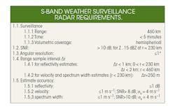
Requirements for 10-cm wavelength (S-band) weather surveillance radars, based on years of experience with the national network of non-Doppler radars (WSR-57), are shown in the table.1 These requirements showcase some of the application-specific metrics that drive range, frequency, antenna size, and gain. They represent the starting point for the system designer, who will also weigh cost and delivery concerns as well as available semiconductor and integration technologies, when considering possible architectures and defining individual component performance targets.
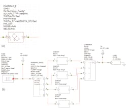
VSS equips system designers with the capabilities needed to convert these requirements into hardware specifications and work out the initial design details. Starting with the phased-array configuration, VSS is able to represent thousands of antenna elements with a single model. This enables the antenna design team to quickly produce radiation patterns with basic array properties, such as number of elements, element spacing, individual element gain or radiation pattern (imported measured or simulated antenna data), array configuration, and gain taper. The model (Fig. 2a) allows designers to specify the array’s physical configuration based on various standard lattice and circular geometries, as well as custom geometries.
2. A single model can delineate thousands of antenna elements (a), replacing system designs based on individually defined elements (b).
The array behavior is easily defined through a parameter dialog box or data file that contains configuration parameters, such as gain and phase offset, theta/phi angles of incidence, number of elements in both X/Y locations (length units or lambda-based), spacing, and signal frequency. This model greatly simplifies early exploration of large-scale phased-array configurations and individual antenna performance requirements in comparison with the old method of implementing such a model using basic individual blocks. With the older approach, array sizes were generally limited to several hundred elements, each modeled as a single-input/single-output block (Fig. 2b).
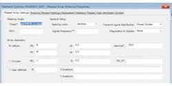
Figure 3 shows a portion of the VSS parameter dialog box used to quickly define an antenna-array architecture utilizing standard or custom geometries. The lattice option allows configuration of the phased array in a lattice pattern, which is configured using the number of elements along the X and Y axes (NX and NY), element spacing along these axes (dx and dy), and gamma (the angle between these axes).
3. Shown is the portion of the phased-array parameter dialog box that contains geometry configuration options, including lattice, circular, and user-defined configurations.
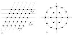
Setting gamma to 90° results in a rectangular lattice, while setting it to 60° creates a triangular lattice. Any positive value for gamma may be used to configure the lattice, while the circular option enables configuration of circular phased arrays with one or more concentric circles. The number of elements in each concentric circle and the radius of each circle can be defined as vectors by variables NC and R. Examples of lattice and circular array configurations are shown in Figures 4a and 4b.
4. These illustrations depict lattice (a) and circular (b) array geometries for phased arrays.
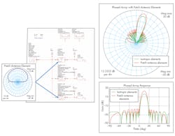
To demonstrate some of the capabilities of the phased-array model, an example project was constructed showing two 15-×-5 element arrays operating at 2.99 GHz (Fig. 5). One model represents an array of lossless isotropic antennas defined simply by setting the antenna gain to 0 dBi, while the elements of the other array utilize a data set containing the radiation pattern of a single simulated patch antenna. Both arrays use a lattice configuration with half-wavelength spacing between elements and uniform gain tapering.
5. These two 15-×-5 element phased arrays are based on isotropic and patch-antenna radiation patterns, respectively. Theta angle is set to 15°.
For the simulation shown, the steering angle (theta) was set to 15°. Note that the antenna and phased-array blocks support specifying the signal direction using U/V coordinates as well as theta/phi angles.
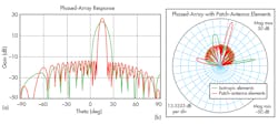
The VSS array model provides antenna designers with a rapid and straightforward tool to observe key antenna metrics. One can examine the main beam and side-lobe behavior as a function of any number of variables, including array size (Fig. 6a) and configuration, gain versus steering angle, and the occurrence of grading lobes as a function of element spacing and/or frequency (Fig. 6b). The element spacing was increased from 0.5λ to 0.95λ to demonstrate how array spacing affects side-lobe growth.
6. Shown are radiation patterns for 15-×-5 and 30-×-5 arrays (a), and side-lobe behavior for a 15-×-5 array with an element spacing of 0.95λ at steering angles of 15° and 80° (b).
From these results, the array design team can develop an optimum configuration for the given requirements, such as range and overall array physical size. In addition, the team can provide design targets for the individual antennas and incorporate subsequent antenna simulation results back into the array analysis.
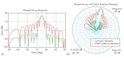
Control of the amplitude excitation through gain tapering is often used to control beam shape and reduce the side-lobe levels. A number of commonly used gain tapers are implemented in the phased-array block. Gain-taper coefficient handling defines whether the gain taper is normalized or not. If it is, the taper is normalized to unit gain. Standard gain tapers implemented in the phased-array model include Dolph-Chebyshev, Taylor Hansen, and uniform. The earlier example (15-×-5 element patch array) was re-simulated with Dolph-Chebyshev gain tapering in place of uniform gain tapering, showing the impact on the main beam and side-lobes (Fig. 7). In addition, the user can define custom gain tapers by specifying the gains (dB) and phases for each array element.
7. This figure compares simulation results of the 15-×-5 patch array with uniform and Dolph-Chebyshev gain tapering.
Conclusion
The first part of this series has introduced new capabilities in EDA software to configure the physical attributes (number of elements and element spacing) of a large-scale phased-array antenna, incorporating measured or simulated antenna radiation patterns and defining any gain tapering to manage the antenna gain, directivity, side-lobes, and more. Part 2 of this series will investigate the individual antenna element design, addressing mutual coupling, the impact of element location, and array impairments due to element failure.
Reference
1. https://www.nssl.noaa.gov/publications/mpar_reports/LMCO_Consult2.pdf
About the Author
David Vye
Technical Marketing Director, Cadence
David Vye is the senior product marketing manager for AWR software at Cadence, where he’s responsible for product messaging and positioning in the RF/microwave market. A former editor and business development manager for Microwave Journal, David has held a number of technical and marketing positions throughout the RF/microwave industry. He holds a BSEE from the University of Massachusetts at Dartmouth, with a concentration in microwave engineering.
