Small Cells Challenge Measurement Capabilities
This file type includes high resolution graphics and schematics when applicable.
Wireless communications networks require test equipment that can keep pace with their ever-improving capabilities. By way of example: Fourth-generation (4G) wireless systems, such as Long Term Evolution (LTE), promise peak data download speeds of 100 Mb/s for high mobility communications services. In support of the highest levels of performance possible, modern wireless networks are relying on a growing number of small cell sites to ensure that coverage is consistent throughout a service area. Of course, with the increased number of small cell sites comes an increased need to test and maintain their performance.
In their formative years, wireless communications systems involved cellular radio networks built from multiple base stations. Some base stations were formed from a group of macro nodes, each of which included a radio tower and antenna and their supporting transceivers. Macro base stations or macrocells were designed to cover wide service areas, perhaps as many as 2000 users over a range of 15 miles (20 to 30 km) or more. In such an arrangement, unfortunately, users near the boundaries of macro base stations tend to suffer reduced signal-to-noise (SNR) performance from their handsets as the signal strength from the macro base station decreases.
Such lower-level signals translate into lower data transfer rates in an LTE system, so the design of a modern wireless communications network also includes the option to supplement a macro base station with a number of smaller cells. These smaller cells are used to augment the coverage at the edges of a macro cell’s range, achieving a range of 0.5 miles (1 km) or more. This “cell-within-a-cell” arrangement results in a more complex wireless communications network that presents a challenge to test equipment manufacturers: They are being asked to deliver cost-effective solutions that can nonetheless tackle more complex testing requirements.
Smaller cells may be used for a number of reasons. The availability of smaller cells makes it possible to offload traffic from a macrocell in areas of heavy use, such as at airports, shopping centers, sports establishments, or anywhere else large numbers of users might gather. In such locations, there may be times when there is very little cellular traffic; smaller cells could depower or switch to a low-power state to save energy during these intervals (Fig. 1).
Another use for smaller cells is to service small-office/home-office (SOHO) locations, where a smaller wireless communications cell provides enhanced performance for as few as 16 users. It can help offset the limitation that higher-frequency signals (typically to 2.6 GHz) used by LTE systems do not penetrate the materials of large buildings as effectively as the lower-frequency signals (700 to 900 MHz) of earlier cellular communications systems. The higher-frequency signals can also be subject to areas of poor reception, where macro signals are severely attenuated. To fill in these blank areas, known as dead zones, operators can provide small cells to reinstate service. Small cells are particularly attractive near cell boundaries, where they can restore high data throughput for users.â¨
The range of small cells spans what formerly were called metro/micro, pico, and femto cells, and also include Wi-Fi access points. These differ in capabilities, range, and the number of simultaneous users supported, but all need to function with the rest of the network so that the overall performance of the system is improved. The resulting complex network, containing both a macro cell and small supporting cells, is known as a heterogeneous mobile network (HetNet).
Earlier second- and third-generation (2G, 3G) wireless networks were carefully planned to ensure adequate coverage and so that there would be no issues with interference between adjacent cells. Small cells in LTE systems must be slotted into what is known as a self-organizing network (SON), and are typically located wherever sufficient power and backhaul series are available. A SON prevents interference by measuring the signal activity in its operating environment, then determining which frequencies and power levels should be used for minimum interference.
Those tasked with testing these smaller cells do not have the luxury of the high-precision laboratory equipment used for compliance testing. Because of the large number of small cells that will be deployed, flexible and portable test equipment that is less expensive than laboratory equipment is more suitable for in-field, on-site testing of small cells. â¨â¨Consider the challenge presented by the wireless environment: The LTE specification includes more than 40 different RF bands spanning the frequency range from 700 to 2600 MHz. In addition, the LTE wireless communications standard encompasses both frequency-division-duplex (FDD) techniques (where different transmit and receive frequencies are used), and time-division-duplex (TDD) techniques (which assign alternating time slots to transmit and receive operations).
As the small cell may be SON-enabled, a suitable portable test solution must be capable of scanning across all possible channels. In such networks, power levels may range from 20 W/channel from a macro base station to just 1 mW/channel from a femtocell. This requires test equipment with a dynamic range of around 70 dB or more.
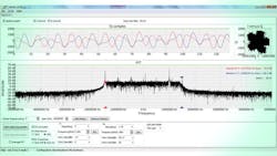
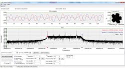
An added complication is that LTE wireless networks employ a number of different bandwidths—including 1.4, 3.0, 5.0, 10.0, 15.0, and 20.0 MHz—and can use multiple different modulation schemes (Fig. 2). Orthogonal-frequency-division-multiplex (OFDM) technology is employed as the signal bearer and the associated access schemes used are either based on orthogonal-frequency-division-multiplex (OFDMA) techniques or single-channel frequency-division-multiple-access (SC-FDMA).
OFDM uses transmissions that are composed of a large number of subcarriers spaced 15 kHz apart that are each modulated at low data rates. The signals are orthogonal to each other so there is no mutual interference, and each carrier contains part of the overall data pattern. The simplest modulation technique uses 2 b/symbol and quadrature-phase-shift-keying (QPSK) modulation, where the carrier can assume one of four different phases at a single amplitude level. QPSK supports low-data-rate transfers and is the default method used under poor signal conditions.
Whenever possible, LTE modulation can be ramped to the use of 64-state quadrature-amplitude-modulation (64QAM) technology, where the phase is shifted to one of multiple different angles and amplitudes to define different bit locations in the constellation and the data carries 6 b/symbol. QAM provides a spectrally more efficient modulation scheme, but only under good SNR conditions. Wideband code-division-multiple-access (WCDMA) signals using a pair of 5-MHz-wide radio channels were introduced as part of 3G wireless communications technology. Such signals are based on code-division techniques that require complex baseband processing to encode and decode.
WCDMA transmissions are also included in the specifications for LTE wireless networks, and can be transmitted as part of the modulation scheme. LTE systems allow users to negotiate the modulation scheme depending on the SNR; as a result, transmitted RF/microwave signals in multiuser parts of these systems can grow quite complex (and quite challenging to measure with portable test equipment).
In support of growing demands for increased data throughput, wireless networks including LTE systems are adopting multiple-input, multiple-output (MIMO) antenna schemes. This is an approach that employs two or more antennas separated by some physical distance. MIMO techniques improve spectral efficiency and achieve a diversity gain that improves link reliability.
MIMO signals can provide robust performance, even under conditions of signal fading and interference or under multipath transmission conditions where the signals reflect off buildings, forming distorted signals at a cell site receiver. Multiple antennas, by careful arrangement of the signal phases sent to each element, can provide a composite signal with a beam-forming capability that can “illuminate” a user with a strong signal.
This file type includes high resolution graphics and schematics when applicable.
Test Solutions
This file type includes high resolution graphics and schematics when applicable.
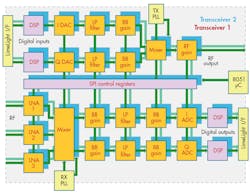
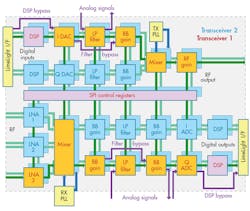
For developers of portable cellular test equipment, a dual transceiver semiconductor device available from Lime Microsystems, model LMS7002M, provides a great deal of flexibility for these in-field wireless test challenges (Fig. 3). This field-programmable radio-frequency (FPRF) chip can be programmed within a test instrument, with receive and transmit frequencies set anywhere from 100 kHz to 3.8 GHz. This wide frequency range encompasses all LTE frequency bands.
The integrated circuit’s (IC) receive path includes three low-noise amplifiers (LNAs), and bandwidth and gain are also programmable on the fly and in the field for a great deal of measurement flexibility. The IC includes a received-signal-strength-indication (RSSI) circuitry to aid in spectral analysis of an LTE system.
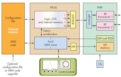
The LMS7002M transceiver IC can process incoming wireless signals and convert them to digital bit streams that represent the in-phase (I) and quadrature (Q) components of the modulated received signals. The transmit and receive frequencies, gain, and bandwidth are all programmed into the device via a serial-peripheral-interface (SPI) connection. The SPI data consists of a 16-b address and 16-b data word. Each element in the FPRF has a unique address, so that SPI data can adjust each of the programmable elements using random access, providing great flexibility for designers of portable LTE test equipment (Fig. 4).
The transceiver IC detects and analyzes a received signal to determine frequency, modulation type, and other signal characteristics. The bandwidth of the FRPF can be adjusted to match an incoming signal, and the decoded I and Q signals can be evaluated for errors by the IC’s companion baseband chip. The FPRF can also transmit across the range of frequencies and modulation schemes designed into the tester. These can be used in loopback mode to evaluate the quality of a wireless link. Transmit frequency, gain, and bandwidth parameters are programmed into on-chip SPI memory to facilitate testing.
The LMS7002M IC has been designed so that both analog and digital signals and key signal-processing elements within the chip can be accessed externally, or else internally bypassed. This provides a test-equipment manufacturer with options to substitute or enhance the filtering using alternative external components, or pass the decoded analog signal through alternative analog-to-digital converters (ADCs) if higher resolution (than available with the IC) is required. Any unused LMS7002M components can be depowered to reduce the device’s power consumption within a portable test instrument.
The LMS7002M includes an on-chip microcontroller running industry-standard 8051 microcontroller code. This simplifies the calibration of the chip in a test instrument, which otherwise would involve complex interactions with the baseband logic. The microcontroller calibrates DC offset, the transmit/receive lowpass filter bandwidth tuning, transmit local-oscillator (LO) leakage feedthrough, IQ gain, and phase mismatch in both transmit and receive signal chains, as well as handling on-chip resistor and capacitor calibration. To supplement the calibration functions, internal RF loopback paths can be enabled to test functionality as part of the IC’s built-in-system-test (BIST) capability.
The FPRF is controlled by an additional baseband chip. This is typically a field programmable array (FPGA), such as a Cyclone V SE for cost-sensitive testers or an Arria V SX for high-performance test solutions—both FPGAs offered by Altera Corp. The function of the baseband chip is to encode or decode the I and Q data streams and to program the FPRF via the SPI interface.
The 32-b ARM cores provide an integrated facility that can interface with the logic fabric or run external code. For example, the logic fabric, memory, and digital-signal-processing (DSP) elements can be configured to perform discrete Fourier transforms—either in the form of Fast Fourier Transforms (FFTs) or Discrete Fourier Transforms (DFT) and forward error correction (FEC)—and generate the modulation patterns for MIMO techniques. These can be configured as required by the ARM microprocessor cores on the transceiver chip, which can initiate the required combination of functions.
The FPGAs are configured upon power up. The configuration file is typically held in an external nonvolatile memory (NMV), such as flash memory, which programs both the logic fabric and the ARM cores. The ARM executable file will typically also be stored in NMV. The NVM can also hold a copy of the SPI configuration data for the FPRF. This data provides a simple way for the processor to store and access the address and data for programming frequency, bandwidth, gain, and DSP elements on the FPRF. This capability allows a test equipment manufacturer the opportunity to update the NVM with new firmware files in the field when adding new capabilities, supporting new standards, or correcting problems, such as programming mistakes (“bugs”).
In terms of creating code, Altera fully supports the Open Computing Language (OpenCL) software. OpenCL allows programmers to quickly exploit the parallel architecture of an FPGA. It enables kernel code to be emulated and debugged, pinpoints performance bottlenecks, and profiles and recompiles programming to a hardware implementation.
Test equipment manufacturers can, for example, use one core to form an interface with a test instrument control panel, and the second core to control the FPGA fabric to the required modulation and the FPRF via the SPI interface. An instrument control panel can present the results as graphical displays of the FFT or as a spectral constellation; the core can compute statistics, such as bit error rate (BER), with the modulation being detected or the number of calls dropped.
Paul Dillien, Owner
High-Tech Marketing, 3 Woodside Dr., Hermitage, Berkshire, RG18 9QD, United Kingdom
This file type includes high resolution graphics and schematics when applicable.
