Compact LNA Drives 2.5-GHz Base Stations
This file type includes high resolution graphics and schematics when applicable.
Low-noise amplifiers (LNAs) are essential to many communications systems, such as cellular communications networks. Achieving low noise figures requires determining such parameters as the optimum impedance matching points, such as for Gopt and conjugate S*11 impedance matching points, for active devices. Balanced LNAs were developed in the 1960s by finding transistor amplifiers’ noncoinciding noise Gopt and conjugate S*11 matching points,1,2 achieving low mismatches by self-cancellation of the reflected energies in quadrature 3-dB couplers (also known as the 90-deg. or hybrid couplers) employed in the LNA design. By assuring good impedance match, a LNA’s constituent amplifiers can then be tuned for minimum noise.
Although an isolator can perform the same function, the cost is comparatively higher. Additionally, a balanced LNA configuration improves upon the reliability, linearity, and bandwidth of its single-ended counterpart and is inherently self-stabilizing (i.e., high stability, both in-band and out of band, is possible even when it is constructed from two potentially unstable amplifiers).3 However, a balanced LNA needs twice the current and components of its single-ended counterpart.
Furthermore, the quadrature couplers represent an additional cost and occupy substantial printed-circuit-board (PCB) space, especially for distributed implementations, and their insertion losses degrade amplifier noise figure (NF), gain, and output power. If commercial drop-in couplers are used, their RF performance levels are generally proportional to their cost and size. More critically, a balanced LNA’s doubled size and weight diminish its viability as a tower-mounted amplifier (TMA) in confined spaces atop cellular towers.
Three broad approaches to miniaturizing a balanced LNA are (a) shrinking the couplers,4,5 (b) integrating the couplers into the amplifying device monolithically6 or in hybrid form,7 and (c) integrating dual amplifiers in either hybrid form8,9 or monolithic form.10,11 However, TMAs also require cutting-edge performance, and this is an obstacle to miniaturization.
Many TMA-centric balanced LNA designs of the past decade have been based on discrete devices,4,5,12,13 but these require a large number of supporting components. To achieve significant reduction in size and component count, dual amplifiers, biasing, and shutdown functions have been integrated into a monolithic microwave integrated circuit (MMIC) and then combined with miniature couplers to create a high-performance, compact 2.5-GHz balanced LNA. The design’s viability as a TMA is contingent upon meeting a number of critical specifications: a sub-1-dB noise figure, 17.6-dB gain in a single stage, better than 18-dB input match, +30-dBm output third-order intercept point (OIP3), and unconditional stability. This may also be the industry’s first dual-amplifier design with integrated shutdown function.
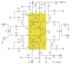
The compact GaAs MMIC comprises dual amplifiers, electrostatic-discharge (ESD) protection, adjustable active biasing, and shutdown functions (the yellow box in Fig. 1). The proximity of the bias function to the amplifier on the same chip also beneficially stabilizes the operating current against gate threshold voltage and temperature variations. For chip fabrication, a proprietary 0.25-μm enhancement-mode pseudomorphic high-electron-mobility-transistor (ePHEMT) process technology on a 6-in. wafer was selected because it best matches the cost-versus-performance requirements. Because this process technology has previously enabled a single-ended LNA to achieve a 0.7-dB NF at 2.5 GHz,14 a balanced design with sub-1-dB NF was anticipated after factoring in about 0.2-dB coupler loss.
The semiconductor process has relatively high transition frequency (fT) and peak transconductance (greater than 30 GHz and about 615 mS/mm, respectively) which should provide the leverage to meet the target gain with a single amplifier stage. Additionally, this process technology’s stable linearity down to 2 VDC drain-source voltage (VDS)15 is beneficial for a cascode arrangement where each transistor only sees one-half the supply. The MMIC is assembled into a 16-pin 4 × 4 × 0.85 mm quad-flat-no-lead (QFN) package using conventional lead-frame wire bonding technology.
This file type includes high resolution graphics and schematics when applicable.
Hitting The Target
This file type includes high resolution graphics and schematics when applicable.
The target 17-dB gain can be achieved with either a cascade of two common source stages or one cascade stage. The latter arrangement was selected for its lower current—i.e., the cascade configuration’s series-connected transistors consume one-half the current of a cascade configuration. The cascode configuration is biased by connecting the upper gate to a resistor divider, while the lower gate is connected to active bias via off-chip inductors L1 and L2. On-chip inductors were not used in these positions since they cannot meet the low RF loss characteristics of off-chip inductors as needed to meet the target NF performance.
In addition to supplying bias, these inductors form highpass networks (in conjunction with capacitors C3 and C16), to roll off excessive low-frequency gain. These input networks need not perform impedance transformation because the ePHEMT device periphery and source inductance Ls have been optimized for impedance matching and low noise in the 2-to-4-GHz band. Likewise, internal prematching by the drain inductance, Ld, simplifies the output networks, L3-C9 and L4-C19.
The on-chip shutdown circuit consists of a transistor switch in series with the active bias. Shutdown is initiated by applying high logic (≥2 V) at Vsd1/2 to open the switch. Conversely, a low logic signal—i.e., Vsd1/2 ≤ 500 mV)—enables the amplifiers. The transition from normal operation to shutdown takes less than 32 ns if the large (≥ 0.1 μF) decoupling capacitors—C8, C22, C23, and C24—are omitted. However, these capacitors are generally recommended because they prevent low-frequency instability and dampen supply transients.
Although the monolithic integration of Lange couplers can achieve the smallest circuit dimensions, the resulting noise figure (e.g., about 7 dB,6) is too high for TMA applications. For this reason, the signal splitting and combining functions in the current design were performed using commercially available surface-mount couplers, X1 and X2. These backward-wave couplers are fabricated on high-dielectric-constant ceramic substrates to achieve compact dimensions: They are about halfway in size between Lange and branch-line couplers. The 2.6-GHz versions of these couplers have enough bandwidth to straddle Fourth-Generation (4G) WiMAX and cellular Long-Term-Evolution (LTE) bands.
To minimize input loss, a larger (6.4 × 5.1 mm) coupler is used at the input port, while a smaller (2.0 × 1.3 mm) coupler is used at the output port to save space and cost. To ensure that a better than 18-dB input match can be consistently met in volume production, controls were instituted on the two most critical parameters: (a) correlating the amplifiers’ input match to |S11a - S11b| < 0.025 dB and (b) specifying an input coupler with better than 23-dB isolation.16 The output coupler is noncritical since the TMA output match requirement is more relaxed.
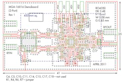
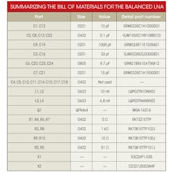
The amplifier PCB consists of a 10-mil-thick layer of RO4350B™ printed-circuit-board (PCB) material from Rogers Corp. with an FR-4 layer added to increase the stack height to 1.6 mm (Fig. 2). RF test connections are made via edge-launched SMA receptacles and the measurements are referenced to these connectors. The occupied circuit area, which is populated mostly with 0402-sized passive components, is 450 × 450 mm. The occupied area can possibly be reduced by about 20% if the empty area between input coupler X1 and the input matching networks (L1 - C3) is removed. The table lists the bill of materials for the amplifier.
This file type includes high resolution graphics and schematics when applicable.
A Closer Look
This file type includes high resolution graphics and schematics when applicable.
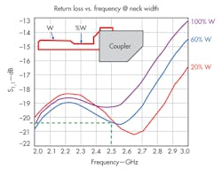
The PCB’s microstrip width (0.58 mm) is nominally dimensioned for an impedance of 50 Ω. However, the traces next to the input coupler’s mounting pads are necked down to compensate for the pads’ parasitic capacitances (Fig. 3). Computer simulations show that the 2.5-GHz input match can be improved by narrowing the trace width to 60% of its nominal value.
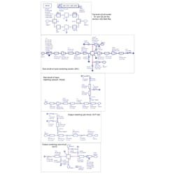
For circuit simulation, the design is modelled using a two-level nested hierarchy (Fig. 4). The upper level consists of blocks representing the MMIC, the signal dividing/combining, and the impedance-matching functions. Each of the dual amplifiers, Q1 and Q2, is represented by an identical set of scattering (S) parameters (.s2p). The device .s2p was previously extracted from a MMIC sample mounted on a test fixture of similar PCB material and thickness, using a thru-reflect-line (TRL) technique to compensate for the fixture.
The device’s noise and linearity [third-order intercept point (IP3)] parameters were also extracted on the same test fixture using automated source and load-pull tuners. The minimum noise figure, NFMIN, of about 0.4 dB is particularly challenging to extract because it is very close to the combined loss of the tuner, cables, and connector adapters. The inductors and couplers are modelled with their manufacturers’ .s2p data. Other passive components are modelled using their equivalent-circuit values, including first-order parasitic values.
This file type includes high resolution graphics and schematics when applicable.
Assessment
This file type includes high resolution graphics and schematics when applicable.
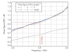
The prototype was evaluated with a +4.8-VDC supply voltage and 2.5-GHz nominal test frequency and found to meet the target sub-1-dB NF at the design frequency. The experimental NF was found to be 0.95 dB at midband, with negligible variability in NF (<0.05 dB) for five samples over a 1-GHz span. The predicted NF follows the same trend as the measured NF, but with value that is lower by about 0.3 dB. This discrepancy is probably due to a modelling error, since the device’s NFmin is close to the measurement limit of the noise characterization equipment.
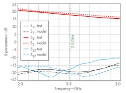
The design capably meets the TMA’s gain and input match requirements. The experimental gain is 18 dB at midband (Fig. 6). The predicted gain is in good agreement with the measured over a 1-GHz span. The experimental input and output return losses are 19 and 17 dB, respectively. In theory, optimum matching should occur at the center frequency of the couplers. The experimental input match for the couplers is optimum at 2.6 GHz, which coincides with the input coupler’s center frequency. The best output match is at 2.3 GHz, however, which does not coincide with prediction (probably due to coupler tolerance). The return-loss amplitude is primarily a function of the coupler’s isolation, although how identical the amplifiers are—as well as discontinuities in the microstrip transmission lines—can contribute to variations in return-loss amplitude.
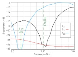
Because the amplifier behaves like a nonreflective attenuator during shutdown, an LNA bypass switch can be potentially eliminated. When the MMIC shutdown is activated, the circuit exhibits 26-dB attenuation, 26-dB input return loss, and 10.5-dB output return loss at 2.5 GHz (Fig. 7). Matching remains good in shutdown mode because reflections from the unpowered amplifiers are self-cancelled in the couplers. The 2.5-GHz output match is worse than expected because the minimum output return loss shifts to 2.15 GHz, possibly because of coupler tolerance. Because of the good match during shutdown, an LNA bypass switch is not required to prevent aerial or filter detuning.
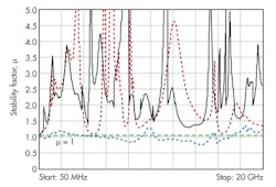
The fabricated balanced LNA is unconditionally stable. Both modelled and measured stability factors, μ, exceed unity from 50 MHz to 20 GHz (Fig. 8). The accuracy of the simulated μ is poor above 3 GHz since the simple equivalent circuits used to model the amplifier’s passive components do not account for the higher resonances above about 3 GHz. What is remarkable is the potential instability of the constituent amplifiers, as indicated by less than unity μ from 7 to 18 GHz, although the balanced topology’s self-stabilizing promise is validated in this design. It is also remarkable that the frequency range where stability is improved, from 7 to 18 GHz, is well above the couplers’ passbands.
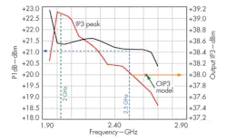
This amplifier design has sufficient linearity to operate reliably in a cellular tower’s noisy RF environment. The 2.5-GHz experimental OIP3 is +38 dBm, about 1-dB lower than the 2.0-GHz peak (Fig. 9). The OIP3 peaks away from 2.5 GHz because the amplifiers’ output networks are tuned for maximum gain. At the expense of reduced gain, it should be possible to improve the 2.5-GHz OIP3 to about +39 dBm by matching for linearity. The OIP3 simulated with load-pull data agrees well with the experimental results, with less than 0.2 dB error at 2.6 GHz. The linearity figure of merit calculated from the ratio of OIP3 to DC power is about 12.4. The midband gain compression point, P1dB, is +21.1 dBm. A high P1dB implies immunity to strong blockers (adjacent channel interference).
Among GaAs MMICs intended for balanced cellular LNA applications, this design has one of the smallest footprints, at 16 mm2. With three functions on the device, the area per function is only 5.3 mm2 compared to previous work7-10 with footprints ranging from 16 to 419 mm2, and even a MMIC footprint of only 16 mm2 at Avago for a single-function device.11 The current design is also the only MMIC cellular LNA with an integral shutdown function.
This design has demonstrated the best performance-to-size ratio among TMA-capable balanced LNAs in the 2-to-3-GHz range. Comparison of different designs can be facilitated by a figure of merit (FOM), such as LNAFOM = OIP3 9mW)/PDC (mW) × NF (dB).17 The current design has an LNAFOM of 13.2. In comparison, designs with large couplers8,9,12 have the highest LNAFOMs but also occupy large PCB areas. The current design combines high performance and compactness—a high value of LNAFOM per unit area.
The proposed balanced LNA design successfully marries high performance and small size, usually conflicting TMA requirements. It achieves substantial reduction in component count by integrating dual amplifiers, bias regulators, and shutdown circuits in a MMIC. When the highly integrated MMIC is coupled with miniature hybrid couplers, the balanced LNA’s PCB size can be significantly reduced. This MMIC’s low-noise performance allows input coupler loss to be traded off for size reduction. A bonus feature of this balanced LNA is the good impedance match during shutdown, which may eliminate the need for switches to bypass the LNA during shutdown. This new design may overcome traditional barriers to the use of balanced amplifier topologies in TMAs.
Acknowledgments
The author wishes to thank H.A. Zulfa, W.H. Chiok, and R. Chuah for the MMIC design and characterization, M.D. Suhaiza and S. Punithevati for assembling the prototypes, and S.A. Asrul and the management of Avago Technologies for approving the publication of this work. Anaren Communications (Suzhou) provided the couplers at no charge.
Chin-Leong Lim, Engineer
Avago Technologies, 11900 Bayan Lepas, Penang, Malaysia; (604) 610-2525.
This file type includes high resolution graphics and schematics when applicable.
References
This file type includes high resolution graphics and schematics when applicable.
1. M. Eisele, R.S. Engelbrecht, and K. Kurokawa, “Balanced Transistor Amplifiers for Precise Wideband Microwave Applications,” IEEE International Solid-State Circuits Conference, February 1965.
2. R.S. Engelbrecht and K. Kurokawa, “A Wideband Low Noise L-Band Balanced Transistor Amplifier,” Proceedings of the IEEE, Vol. 53, No.3, March 1965, pp. 237-247.
3. Steve C. Cripps, RF power amplifiers for wireless communications, Artech House, Norwood, MA, 1999, Section. 10.2 “Balanced amplifiers.”
4. J.S. Mandeep and H. Abdullah, “A compact, balanced low noise amplifier for WIMAX base station applications,” Microwave Journal, November 2010.
5. A.F. Osman and N. Mohd. Noh, “A design for SDR radio using balanced amplifier topology,” 4th Asia Symposium on Quality Electronic Design, 2012.
6. S. Seo, D. Pavlidis, and J.S. Moon, “Wideband balanced AlGaN/GaN HEMT MMIC low noise amplifier,” Electronics Letters, Vol. 41, No. 16, August 2005.
7. B. Jensen, “Build LNAs with an integrated approach,” Microwaves & RF, December 2002.
8. T. Chong, “A Low-Noise, High-Linearity Balanced Amplifier in Enhancement-mode GaAs pHEMT Technology for Wireless Base-Stations,” Proceedings of the European Microwave Conference, Paris, France, October 2005.
9. T. Chong and S. Rendava, “Design and Performance of a 1.6-2.2-GHz Low-Noise, High Gain Dual Amplifier in GaAs E-pHEMT,” Asia-Pacific Microwave Conference, Suzhou, China, December 2005.
10. Ommic application note, “CGY2105XHV/AB2500 2.5-2.7 GHz balanced low noise amplifier application board.”
Related Articles
• LNA Boosts 6 To 20 GHz
• Variable-Gain LNA Reaches 26 GHz
• Broadband Radio’s LNA Shoulders Harmonic Rejection To 20 dB
11. Avago Technologies, Application Note 5442, “LNA Design with the MGA-17516 Matched Pair, Low Noise Amplifier.”
12. I. Piper, S. Seward, A. Ward, H.P. Hostergaard, and S. Tozin, “Balanced LNA suits cellular base stations,” Microwaves & RF, April 2002, pp. 70-80.
13. J.-L. Olvera-Cervantes, A. Corona-Chavez, R. Chavez-Perez, H. Lobato-Morales, J.-R. Ortega-Solis, and J.-L. Medina-Monroy, “A wideband quadrature power divider/combiner and its application to an improved balanced amplifier,” Progress In Electromagnetics Research C, Vol. 34, 2013, pp. 29-39.
14. Avago Technologies, Application Note 5479, “MGA-635P8 GaAs ePHEMT MMIC 2.5-GHz low-noise amplifier with superior noise and linearity performance.”
15. J. Madden, “Low voltage operation of GaAs power amplifier,” Microwave Journal, September 2006, pp. 130-134.
16. Anaren Co., Product Specification, “X3C26P1-03S hybrid coupler,” Rev. C.
17. “IMS 2011 student design competitions,” IEEE Microwave Magazine, February 2011, pp. 98-99.
This file type includes high resolution graphics and schematics when applicable.
