Design Method Predicts RF Oscillator Noise
This file type includes high-resolution graphics and schematics when applicable.
Noise plagues most RF/microwave systems at some level. The majority of system-level designers aim to achieve the highest signal-to-noise ratios (SNRs) possible to ensure optimum reception of signals in, say, receivers. Minimizing noise usually starts with the signal source, whether it’s an oscillator or an oscillator with a phase-locked loop (PLL) in a frequency synthesizer.
Designing a quiet source requires paying close attention. But, as will be shown with the design of a low-noise, 2-GHz microwave oscillator, it’s possible to better understand active device noise mechanisms through rigorous analysis. One benefit of this analysis is an opportunity to design and construct a stable, low-noise oscillator that operates well within the linear region of its active device, a gallium-arsenide (GaAs) field-effect transistor (FET).
The 2-GHz oscillator is based on a clamped, linear 40-GHz Schottky-barrier diode approach, operating within the linear region of a small-signal GaAs FET. The oscillator design is able to drive a 50-⦠load with low-noise 2-GHz energy, relatively free of harmonic distortion. The oscillator design was analyzed with a discrete Fourier transform (DFT) program featuring a dynamic range of greater than 260 dB.
As a rule, microwave oscillators will exhibit some level of harmonic distortion when driving a 50-⦠load. Ideally, harmonic, subharmonic, and spurious signal distortion can be minimized without degrading oscillator single-sideband (SSB) phase noise. Traditionally, signal source harmonics and phase noise have been analyzed by means of harmonic-balance frequency-domain methods to track the steady-state nonlinear responses at higher frequencies. But by using the time domain, followed by a novel DFT analysis method, excellent results were achieved in the analysis of the 2-GHz GaAs FET oscillator.
Test Setup
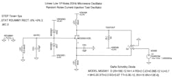
In the novel oscillator analysis approach, two identical oscillators were constructed for simulation purposes. They were injection locked at their FETs’ gates, so that both oscillators would remain in phase relative to each other. One of the oscillators was considered a reference and the other the device under test (DUT), with a random noise source injected into the DUT. The output of the DUT oscillator (TESTOUT) is then subtracted from the output of the reference oscillator (REFOUT), followed by a DFT to produce the desired results.
The analysis method has been capable of measuring extremely low noise levels in the nanovolt range. The random noise source (V1) drives a transconductance block (G2) with a value of 1.0, injecting random current into the drain and source of the DUT. Multiple simulation runs are performed, with each run using random-noise-generator “seed” values to produce a series of random voltages that are unique for each simulation run. The random noise generator operates with one step every 1.000055 ns, with peak values of ±1 nV, which in turn drive the transconductance block (G2).
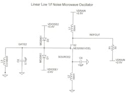
The negative resistance seen at the gate of the oscillator is obtained by providing a capacitive load at the source of each FET at 2 GHz. The inductors in the FET sources act as a bias tee, providing only dc bias to the device. The diodes in each FET’s gate are Schottky-barrier GaAs diodes rated at 40 GHz. They provide a small load to the tank circuit while biased at low forward voltages.
The linear gain of the oscillator at 2 GHz is the value of the load resistance (50 â¦), divided by the capacitive reactive loading at the FET source. The capacitor’s value in the source of the FET is chosen to provide a negative resistance as seen at the FET gate and the desired amount of linear gain for oscillation.
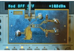
Figure 1 shows the hardwired test fixture for evaluating the oscillator’s performance, fabricated on FR-4 printed-circuit-board (PCB) material using chip and discrete circuit elements. The unused ports were terminated into the characteristic 50-⦠system impedance to protect against static discharge when the photograph of the fixture was being taken.
The Results Are In
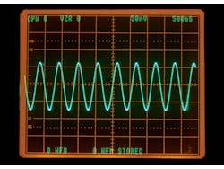
Figure 2 shows the output of the test oscillator in the text fixture on the screen of a commercial sampling oscilloscope. The traces reveal very low harmonic distortion into 50-⦠impedance.
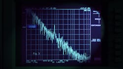
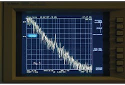
To evaluate the test oscillator’s phase noise, a commercial signal analyzer from Agilent Technologies (now Keysight Technologies) was used to measure the plot of Fig. 3 with reference level at –40 dBc. For comparison, a voltage plot of the reference oscillator (Fig. 4) was produced with the assistance of the TopSpice computer-aided-engineering (CAE) software, a mixed-signal, analog/digital circuit-design program available from a variety of online sources, including Penzar.
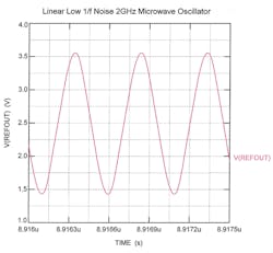
The time-domain plot of Fig. 5 shows low-noise characteristics similar to those of Fig. 3. Again, the reference oscillator is identical to the test oscillator, with the difference being that the test oscillator is being driven by a random noise source with zero mean deviation.
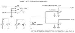
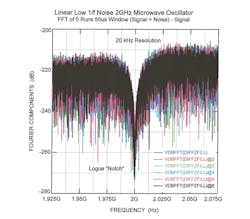
A combination of TopSpice (a PC version of SPICE modeling software) and a custom FFT program was used to produce a fast Fourier transform (FFT) display of the test oscillator for five runs across a 50-µs window across a frequency range of 1.925 to 2.075 GHz with 20-kHz resolution (Fig. 6). Similarly, Spice was employed in the design of the phase-locked injection-lock circuitry used to drive the gates of both the reference and test oscillator circuits (Fig. 7).
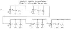
The computer simulation reveals second-harmonic distortion is extremely low, 42 dB removed from the fundamental frequency amplitude level. Third-harmonic distortion is –30 dBc from the fundamental-frequency level. To reduce aliasing and higher-order harmonic levels in the 2-GHz oscillator simulation, a five-stage, 22.7-GHz filter was included in the simulation results (Fig. 8).
Overall, the noise components from the computer simulation are more than 210 dB removed from a 0-dB reference, for impressive performance achieved with the aid of comparing performance for the two 2-GHz oscillators when injecting current noise (Fig. 9). Though the analysis technique essentially requires the fabrication of dual computer-model prototypes, it lends itself to low-noise oscillator design and development across a wide range of frequencies.
