RF MEMS Switches Are Primed For Mass-Market Applications
This file type includes high resolution graphics and schematics when applicable.
Historically, RF switches have fallen into two categories: electromechanical relays and semiconductor-based devices. Examples of the latter include components using PIN diodes, gallium-arsenide (GaAs) FETs, and silicon-on-insulator (SOI) or silicon-on-sapphire (SOS) transistors as the active switching devices. Although such devices offer reliable performance, they can be expensive. In addition, they have limited lifetimes. Fortunately, a new option has arrived in the form of the RF microelectromechanical-systems (MEMS) switch. For commercial-bound RF MEMS integrated circuits (ICs), novel solutions have emerged to enable reliable packaging, smaller size die, improved metal-contact switching, better and tighter control of the MEMS RF process, and longer lifetimes.
RF MEMS offer a very high figure of merit (FOM) together with high linearity and low power consumption. The FOM is a function of a switch’s on-resistance (when it is closed) and its off-resistance (when it is open). In the case of RF MEMS, the FOM is orders of magnitude higher than other switching technologies. In addition, it features significantly higher isolation or lower insertion loss at any frequency. These systems also are compatible with existing semiconductor manufacturing processes, which can lead to high volumes and lower costs.
“The main technical challenge for the RF MEMS community is in transitioning from prototype manufacturing to consistent larger-scale manufacturing,” notes Charles L. Goldsmith, President of MEMtronics. “The cost of making small quantities runs high, which limits the ability to demonstrate products for low-cost consumer items like mobile phones. It is difficult to maintain repeatability and consistency when manufacturing on a large scale.” MEMtronics uses wafer-level micro-encapsulation in its manufacturing process.
Gabriel Rebeiz, a pioneer in RF MEMS technology who is considered one of its founding fathers, foresees greater use of RF MEMS in aerospace/military, automatic test-equipment (ATE), and ultra-low-power RF-identification (RF ID) applications. Currently Professor at the University of California San Diego and the Wireless Communications Industry Endowed Chair, Rebeiz states, “RF MEMS is ready for wide-scale use in fourth-generation (4G) Long Term Evolution (LTE) applications. It is only a matter of time before the number of RF MEMS devices delivered increases and the low-cost issue will be solved.”
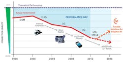
In terms of performance demands, 4G LTE mobile phones comprise one of the more tantalizing markets for RF MEMS. The voice signal quality for such phones has been declining compared to earlier GSM, two-and-a-half-generation (2.5G), and third-generation (3G) phones. Such degeneration is due to greater use of cellular communications and full-screen phones coupled with the evolution to touchscreen technology. As mobile smartphones become smaller and thinner, it is difficult for designers to incorporate the performance-enhancing circuitry required to counter dropped cell-phone calls and raise voice quality (Fig. 1).
1. Voice signal quality for smart mobile phones has been declining due to greater use of cellular communications, the use of full-screen phones, and the evolution to touchscreen technology. This issue has created a need for countermeasures that can be provided by RF MEMS tuning. (Source: Cavendish Kinetics)
“The ratio of the theoretical to the realized RF signal quality has been declining by about 1 dB per year for over a decade,” explains Dennis Yost, Founder and CEO of Cavendish Kinetics. He cites the trend toward thinner form factors for mobile phones, larger screens, expanded frequency bands, and cool software applications as factors in the decline of signal quality. The company is targeting tunable antennas and filters for the front end of 3G and 4G phones as a first step toward many other RF front-end applications. A switched capacitor array for antenna impedance matching with 32 capacitor values is scheduled for release before the end of this year.
Rebeiz adds that tunable RF MEMS filters and antennas will alleviate the present mobile-phone signal loss of 3 to 5 dB in the 700-MHz-to-2.7-GHz band. “You have not seen anything yet: Wait for carrier aggregation and harmonic blocking in the 700-to-2100-MHz range,” he stated in a paper delivered at the IEEE RWW 2013 Conference in Austin, TX this past January.
Roger Grace, President of Roger Grace Associates, is a long-time MEMS consultant and a former RF component designer. He agrees with many of these market assessments on the future of RF MEMS chips: “The primary reason for the lack of success has been the inability for manufacturers to adequately address the need of instrumentation (notably ATE) in the consumer-electronics/phones/tablets sector and create a sufficiently inexpensive packaged device to be integrated into systems.”
Grace adds, “I expect true commercialization for RF MEMS switches as early as the 2014/2015 timeframe, which will be driven—in part—by expected positive outcomes in switch reliability developments and low-cost packaging vis-a-vis wafer-level packaging (WLP), as well as through the migration into 200-mm and beyond wafer diameters.” (Here, he cites his “Barriers to Successful Commercialization of MEMS: The 2012 Industry Commercialization Report Card,” which is available on the firm’s website.)
Jeffrey L Hilbert, President and Founder of WiSpry, Inc., cites market estimates for antenna-tuning applications using RF MEMS ICs at about $500 million a year in the 2015 timeframe—growing to $1.2 billion by 2017. “While RF MEMS-enabled products are capable of servicing all of this market segment, other technologies will also be used for antenna tuning,” Hilbert notes. “Close behind antenna tuning, you will see tunable antenna filters and power amplifiers in smartphones.”
MEMS For Smartphones
Most experts agree that the smartphone market will be the driving force and the initial high-volume driver for RF MEMS ICs. WiSpry has been shipping large-volume switched-capacitor switches (reportedly over 1 million units so far). It fabricates its products on a mainstream 180-nm, RF-metal-CMOS process on 8-in. wafers as single die. To minimize testing costs, the firm uses standard IC ATE equipment. Its multiband (800-to-2200-MHz), low-loss (0.3-dB) chips measure just 3.5 x 4.2 x 1.1 mm. They are manufactured using standard wafer-level chip-scale packaging (WLCSP). Early this year, WiSpry introduced the WS1035, an LTE-optimized, tunable digital-capacitor array that offers a 60% reduction in board space (Fig. 2). The chip has been used in Samsung’s smartphones since late 2011.
2. Reportedly, over 1 million CMOS RF MEMS switches have been produced by WiSpry for the smartphone market using wafer-level chip-scale packaging. The most recent is the WS1035180, an LTE-optimized tunable digital capacitor array that offers a 60% reduction in board space. (Source: WiSpry, Inc.)
Cavendish Kinetics is about to enter this market with metal-CMOS, switched-capacitor RF MEMS switches using its proprietary NanoMech technology. That technology uses bare-bump die for flip-chip mounting. Each die is a mere 2 mm2—much smaller than a US dime. The chips are manufactured by encapsulating them inside chip micro-cavities. These microcavities isolate the MEMS moving parts from contaminants, eliminating the extra step normally required for conventional switched-capacitor arrays.
Like other RF MEMS IC manufacturers, Cavendish’s Yost stresses the need to carefully control a chip’s design and process for maximum reduction of costs. “You must control the manufacturing and design processes. How a MEMS IC is built is just as important as what you build,” he summarizes. The firm’s first chips, which are slated for the market by the end of this year, perform antenna impedance matching. Each will have 32 capacitor-value steps in a chip-scale package that is not much larger than a conventional single-value chip. The chips will offer 5-b resolution.
The France-based DelfMEMS is presently sampling RF MEMS ICs for 4G smartphones. It uses a process that has a limited number of masks in 3-μm steps. It targets large-volume, low-cost front-end devices—estimated to cost users about 2 to 2.5 cents/switch throw—in single-pole/single-throw (SPST) and single-pole/double-throw (SPDT) configurations.
“We want to simplify a smartphone front end and its bill of materials,” notes Olivier Millet, DelfMEMS’ Founder and Chief Strategy and Marketing Manager. “Our aim is to provide reliable switching, very low switching time, and a MEMS device that can be integrated using over-molding and bumping techniques.” To achieve this goal, the company is using low-cost chemical mechanical planarization (CMP) for a smaller size switch. It has been working with Tronics MEMS’ foundry facility.
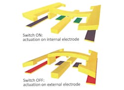
Notably, DelfMEMS uses a patented push-pull, anchorless-membrane MEMS switch structure that it claims is a new approach to ohmic switching (Fig. 3). It can be integrated with capacitors using wafer-level thin-film packaging. The switch is supported by just two pillars. Because it is anchorless, it has no package and temperature dependencies, is ultra-fast, and has no stress concentration. The structure has a small gap, high restoring and contact forces, and offers a controlled switch state.
3. This patented push-pull, anchorless-membrane RF MEMS switch from DelfMEMS is said to offer a new approach to ohmic switching. It can be integrated with capacitors using wafer-level, thin-film packaging. (Source: DelfMEMS)
Military/Aerospace/ATE Applications
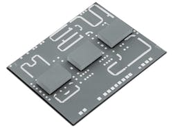
Low-cost RF ICs are not just limited to mass-market 4G smartphones. “Low cost is always an issue for RF MEMS ICs. It is even an issue for the US Department of Defense (DoD), which is becoming more focused on it,” says John Maciel, Vice President and Chief Operating Officer for Radant MEMS, Inc.—a manufacturer of RF MEMS devices for aerospace and military applications (Fig. 4). With the help of DoD DARPA funding, this firm has helped to increase MEMS switch reliability to 1.5 trillion cycles. The company provides band-select switching for various receive and transmit chains and phase shifters. It developed a novel electronically steered antenna with key attributes including low insertion loss, extreme linearity, and a broad bandwidth.
4. This broadband, true-time-delay (TTD), DC-to-20-GHz phase shifter targets military applications. Every cap contains the MEMS switch die for each of the three 2-b elements. (Source: Radant MEMS)
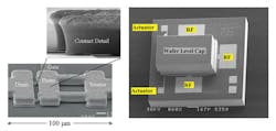
Radant MEMS is continuously developing fully surface-mount-technology (SMT) versions of its chips, which require through-silicon vias (TSVs) and process development. The use of SMT enables the elimination of real estate that is currently employed for bond pads, thereby reducing size and cost (Fig. 5).
5. Shown is an SEM microphotograph of capped die containing a DC-to-18-GHz RF MEMS switch (right), which was obtained through a wafer-bonding process (left). (Source: Radant MEMS)
Last year, semiconductor foundry TowerJazz and the University of California San Diego collaborated on the demonstration of the first 0.18-μm wafer-scale, silicon-germanium (SiGe), BiCMOS wideband (75-to-110-GHz) phased-array transmitter chips. In 5.6 by 6.0 mm, each chip combines the 110-GHz source, amplifiers, distribution network, phase shifters, and high-efficiency antennas on chip. The chip has 16 radiating elements and all of the necessary CMOS control circuits. It is capable of electronic beam scanning of ±40 deg. in all planes.
Test Steps Forward
In the ATE arena, progress continues. As far back as 2009, Omron Corp. introduced a 10-GHz SPDT RF MEMS switch—the 2SMES-01aimed at ATE applications. That 5.2-x-3.0-x-1.8-mm chip has a life expectancy of 100 million operations (0.5 mA at 5.0 VDC resistive load), 30-dB isolation, and 1-dB insertion loss. It can handle up to 10 μW. The switch uses an electrostatic drive mechanism, which combines the desirable effects of high-frequency characteristics of electromechanical relays with the life expectancy generally found only in solid-state relays. It is manufactured on both 5-in. and 8-in. MEMS wafer production lines.
Last year, Advantest developed a 20-GHz SPDT MEMS switch for ATE applications using a 1-μm-thick piezoelectric film. It features low-actuation voltage (12 V), more than 20 dB of isolation, and less than 1 dB of insertion loss. Advantest expects to mass-produce the switch this year. It is available in two sizes: 5.4 x 4.2 x 0.9 mm and 2.9 x 3.4 x 0.9 mm.
According to Dan Hyman, CEO of Xcom Wireless, “The largest roadblock to the ATE market has been sourcing and production quantity, which ties into packaging and manufacturing yield. The higher-volume ATE-component buyers require at least a moderate-volume manufacturing history that is stable and proven sustainable for extended periods of time.”
XCom has supplied a handful of customers with samples of 10-V RF MEMS switches. These switches have not yet been qualified. The company is working on final modifications to the packaging process along with lifetime testing. Hyman says that XCom also is working to satisfy moderate-cost applications in military tactical radios and sensor platforms—both of which are in the early stages of development.
Like the smartphone segment, the military/aerospace and ATE sectors foresee large benefits and many applications from the use of RF IC switch developments. But more work needs to be done to mass-produce these switches to lower costs as well as to increase reliability and lifetime levels. Here, research at the academic level and within industry can be very helpful. Gabriel Rebeiz at the University of California San Diego and many other researchers are spearheading this work. According to Mina Zadeh, Assistant Professor at the University of Michigan’s Electrical Engineering and Computer Sciences Department, “We see exciting developments in RF MEMS technology—not only in reconfigurable band-pass and band-stop filters, but also in metamaterials-based modulators and shutters for infrared and terahertz modulation.”


