This file type includes high resolution graphics and schematics when applicable.
Amplitude control is a critical function in many high-frequency communications and other systems and often handled by a voltage-variable attenuator (VVA). In wireless receivers and transmitters, for example, VVAs can provide automatic gain control. They also can help minimize amplifier gain variations with temperature and semiconductor process variations.1 The π and bridge-T topologies are the most compact of the constant-impedance VVA configurations, since they are realized solely with lumped-element circuit components.2,3
The variable resistances of a VVA design can be approximated with either field-effect transistors (FETs) or positive-intrinsic-negative (PIN) diodes, although the latter will result in an atenuator with higher linearity.4 While the basic π topology requires only three resistive elements, implementing this VVA with three diodes, as it was initially done, results in an asymmetical circuit that is complicated to bias.5,6 Consequently, a revision of the π VVA using four diodes has gained popularity because of its simpler biasing than the three-diode configuration.7,8
A π VVA has a limited frequency range which, according to some reports, reaches a maximum upper frequency limit of 1 GHz.9 Its frequency response is bounded by the maximum attenuation degrading at 6 dB/octave due to signal leakage through the series diodes’ parasitic elements. One way to circumvent this frequency ceiling is to apply parasitic cancellation on the affected diodes. Applying this technique to a π VVA fabricated with discrete components, it was possible to achieve about a 25-dB attenuation range at 3.8 GHz.10
However, the discrete implementation requires many components, and this consumes considerable space. To reduce the component count and size of the VVA from previous designs, the current work extends this technique to a standalone, highly integrated PIN-diode π VVA module. This report describes the design and characterization of a compact, high-performance 3.5-GHz VVA.
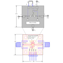
The heart of this attenuator design is a PIN diode VVA circuit in a multi-chip-on-board (MCOB) module.11,12 Measuring 3.8 × 3.8 × 1 mm3, the VVA is contained within a lead-less plastic package that integrates 13 passive devices and 4 diodes (Fig. 1). Two voltage supplies are required to operate the VVA: a control voltage (Vc at pin 4) variable over a range of 0 to +5 VDC and a +2.7-VDC reference voltage (Vs at pin 2). The control voltage is used to adjust the attenuation. The reference voltage, Vs, is used to control the current relationship between the series and the shunt arms. In this way, Vs is used to optimize the VVA’s impedance matching over the attenuation range.
Without parasitic cancellation, the module’s maximum attenuation is a modest 27 dB at 3.5 GHz. The module permits access to the series diodes through pins 5 and 6. Via these pins, an external inductor, L1, can be connected in parallel with the series diodes. At resonance, its inductance and the diodes’ capacitances will cancel, leaving the diodes’ junction resistances in series with the signal path. Therefore, the problem of signal leakage through the parasitic capacitances is eliminated. However, the improvement is narrowband. Although the parasitic cancellation technique is demonstrated on this standalone VVA module, it should be applicable to any π VVA—whether it is a discrete or integrated-circuit (IC) design—as long as the series arm is accessible.
Excluding the connectors, the bill of material (BOM) for this VVA solely consists of two components. Both are mounted on one side of a 10-mil-thick RO4350 printed circuit board (PCB) from Rogers Corp. The component-less side of the PCB is glued to an FR-4 circuit-board layer for rigidity, as well as to increase the stack height to 1.6 mm, so as to suit the edge-mounted SMA receptacles. All measurements are referenced to these connectors and so include connector and PCB losses.
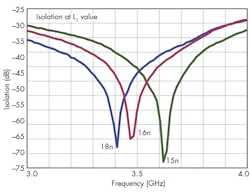
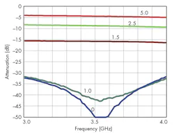
Computer circuit simulations can predict the correct L1 inductance value if accurate circuit models of the inductor, the module, and the PCB are available. Due to the lack of resources to develop these models, it was decided to determine the L1 value using the “cut-and-try” approach. After deciding on a 0603-size wirewound inductor series,13 different L1 values were substituted into the prototype circuit design to gauge the effects. Although the target resonant frequency was 3.5 GHz, the inductance granularity prevents this.
Finally, a inductance value of 16 nH was chosen because the resulting notch it produced was closest to 3.5 GHz (Fig. 2). The spacing between the notches are not consistent with the stated inductance values—this probably points to tolerance in either the inductance or the parasitic capacitance. Ideally, an inductor with tight tolerance should be specified for L1 to minimize variation in the notch frequency. Although a multilayer inductor can be used for a cost savings, it is not recommended because of its higher parasitic capacitance and lower quality (Q) factor compared to a wirewound inductor.
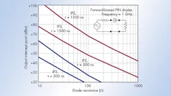
For a VVA that is meant to pass complex, multitone waveforms, linearity can be a bottleneck and a problem when lacking. To understand the linearity performance of a VVA based on diodes requires some background of the diodes’ distortion-generating mechanism. The subject VVA module’s four diodes are forward biased over most of the attenuation range, except at low control voltages (i.e., less than +1 VDC). In the forward-biased condition, distortion is created by RF currents modulating the charge density of the diode’s intrinsic (I) layer.
This file type includes high resolution graphics and schematics when applicable.
A Two-Pronged Approach
This file type includes high resolution graphics and schematics when applicable.
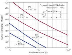
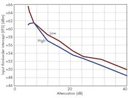
The VVA module employs two techniques to minimize distortion. First, the two series diodes are orientated in the opposite direction to produce out-of-phase distortion so that their even-order distortion will be partially cancelled.14,15 Secondly, the diodes are chosen for a large ratio of carrier lifetime π to on-state resistance.16 These long-lifetime diodes (π = 1500 ns) can improve the VVA’s third-order intercept by more than 30 dB compared to shorter-lifetime (500 ns) diodes (Fig. 3). The long-lifetime diodes require approximately ten times higher operating currents, but this tradeoff is tolerable because intended applications are typically powered powered by mains supplies.
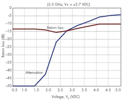
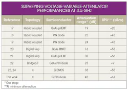
The VVA’s attenuation is adjustable over a 45-dB range at 3.5 GHz. This represents the highest amount of attenuation yet reported in a single VVA stage (see table).17-24 At the maximum control voltage (Vc = +5 VDC), the experimental minimum attenuation is about 4.4 dB (Fig. 4), of which 0.3 dB is contributed by the PCB and connectors. At zero control voltage, a maximum attenuation of about 50 dB is achieved. The attenuation at 3.5 GHz is slightly less than the maximum possible because the notch is offset to 3.52 GHz. Compared to the original circuit, parasitic cancellation improves the maximum attenuation by about 22 dB.
The VVA input and output impedances remain stable over the attenuation range. The return loss measures better than 10 dB over 45 dB of change in attenuation (Fig. 5). The impedance match is best at the attenuation midrange, but degrades toward either end of the attenuation range.
The experimental linearity performance of the VVA surpasses previous figures (see table). At minimum attenuation, the third-order input intercept point (IIP3) exceeds +61 dBm (Fig. 6). This IIP3 is at its highest level because the control voltage (Vc) is at a maximum, hence heavily biasing the VVA’s series diodes. The IIP3 gradually decreases with higher attenuation levels but does not descend below +48 dBm over a 40-dB attenuation range.
In short, using this design approach, the PIN diode π attenuator’s operating frequency can be extended to the microwave range through the use of this parasitic cancelling technique. As this highly integrated VVA module has shown, this compact design can operate at 3.5 GHz using one external component. The design approach is compact and simple and relatively low in cost, but achieves a wide attenuation range with superior linearity.
Acknowledgment
The author thanks Y.M. Fong for designing the VVA module.
Chin Leong Lim, Engineer
Avago Technologies, Penang, Malaysia
References
1. C.L. Lim, “Wideband voltage variable attenuator with few components,” Microwave Journal, December 2011.
2. K.C. Gupta, “Microwave Control Circuits,” in Microwave Solid State Design, 2nd ed., I. Bahl and P. Bhartia, Eds., Wiley, New York, 2003, pp. 683-685.
3. Avago Technologies, application note 922, “Applications of PIN diodes,” 1991.
4. E. Higham, “Distortion in voltage-variable attenuators,” Microwave Journal, December 1999, pp. 86-95.
5. R. Sydow, “PIN Diodes,” in Capacitance Diodes, Tuner Diodes, Diode Switches, PIN Diodes Basics and Applications, ITT, 1976, pp. 55-58.
6. Ulrich L. Rohde and D.P. Newkirk, “PIN Diodes” in RF/Microwave Circuit Design for Wireless Applications,” Wiley, New York, 2000, Section 2-1-3, p. 152.
7. Ray W. Waugh, “A Low Cost Surface Mount PIN Diode Pi Attenuator,” Microwave Journal, Vol 35, No. 5, May, 1992, pp. 280-284.
8. S. Huettner, “Waugh Attenuator,” in Microwaves 101, July 2011.
9. A. Grebennikov, “Attenuators,” in RF and Microwave Transmitter Design, Wiley, New York, 2011, Section 13.4.
10. Avago Technologies, application note 5383, “Improving the maximum attenuation of the HSMP-3816 PI attenuator at 3.8 GHz,” April 2008, www.avagotech.com.
11. Avago Technologies, datasheet, “ALM-38140,” www.avagotech.com.
12. C.L. Lim, “VVA extends BW and dynamic range,” Microwaves & RF, October 2011, pp. 54-62.
13. Coilcraft Industries, document 537-1, “Chip inductors – 0603HP series,” May 2009.
14. R.W. Waugh, “A low distortion PIN diode switch using surface mount devices,” Proceedings of the RF Expo West, February 1991, pp. 455-461.
15. Avago Technologies, application note 1049, “A low distortion PIN diode switch using surface mount devices."
16. R.H. Caverly, “Distortion in RF and microwave control devices,” Microwave Journal, December 1997.
17. Skyworks Solutions, product specification, “SKY12146-321LF: 3.0 – 3.8 GHz, 20 dB variable voltage attenuator,” April 2011, www.skyworksinc.com.
18. Skyworks Solutions, product specification, “SKY12236-11: High IIP3, 2.6 to 5.0 GHz voltage-controlled variable attenuator,” March 2014, www.skyworksinc.com.
19. Valpey Fisher product specification, “VFVA505-200,” 2011.
20. Hittite Microwave, product specification, “HMC603QS16.”
21. E.E. Austin, H. Cebi and J. Yang, “Tackling multi-bit attenuator designs,” Microwaves & RF, March 2012, pp. 91-118.
22. K.W. Kobayashi, A.K. Oki, D.K. Umemoto, S. Claxton, and D.C. Streit, “GaAs HBT PIN diode attenuators and switches,” IEEE Microwave Symposium Digest, 1993.
23. M. Granger-Jones, B. Nelson, and E. Franzwa, “A broadband high dynamic range voltage controlled attenuator MMIC with IIP3> +47dBm over entire 30-dB analog control range,” IEEE Microwave Symposium Digest, 2011.
24. D. Walraven amd E. Franzwa, “RFSA2013 and RFSA2023 broadband high performance voltage-controlled attenuators, Microwave Product Digest, June 2011.
This file type includes high resolution graphics and schematics when applicable.
About the Author

Leaders relevant to this article:
