GaN-On-SiC Devices Power DC To 18 GHz

This file type includes high resolution graphics and schematics when applicable.
Gallium nitride (GaN) semiconductor devices have captured the attention of solid-state circuit designers in recent years, owing to their high power levels from relatively dense circuits at RF/microwave frequencies. TriQuint Semiconductor has added to the interest by fabricating GaN devices on silicon-carbide (SiC) substrates, resulting in rugged, reliable devices capable of high output-power levels at microwave frequencies. The firm’s latest additions to its lines of GaN-on-SiC high-electron-mobility-transistor (HEMT) discrete power transistors includes models TGF2023-2-01, TGF2023-2-02, TGF2023-2-05, TGF2023-10, and TGF2023-2-20. All are chip devices designed for different power gain and output levels from DC to 18 GHz in commercial, industrial, and military applications.
The company, which released its first GaN-on-SiC process in 2008, has applied GaN semiconductor technology to achieve higher power densities and efficiencies at higher frequencies than possible with other semiconductor device technologies. GaN devices boast high breakdown voltages compared to other high-frequency device technologies, such as gallium arsenide (GaAs) and silicon CMOS devices. This latest line of broadband power devices s suitable for defense and aerospace systems and for broadband communications applications.

The lowest-power model in the lineup is model TGF2023-2-01 (Fig. 1), designed for 6 W output power from DC to 18 GHz. It delivers +38 dBm nominal saturated output power at 3 GHz with 18-dB nominal power gain at that same test frequency. The discrete GaN-on-SiC HEMT achieves 71.6% maximum power-added efficiency (PAE), operating with quiescent current of 25 to 125 mA and drain voltages of +12 to +32 VDC. The device, which measures 0.82 × 0.66 × 0.10 mm, draws 400 mA typical current under RF drive condition, with maximum drain voltage rating of +40 VDC and maximum drain current of 1.25 A. As with the other new GaN-on-SiC devices in this family, the TGF2023-2-01 is lead free and RoHS compliant. It can handle maximum CW input power to +31 dBm.
Next in power is model TGF2023-2-02, with 12 W output power from DC to 18 GHz. This GaN-on-SiC HEMT measures 0.82 × 0.92 × 0.10 mm but achieves +40.1 dBm nominal saturated output power at 3 GHz. It also provides 73.3% maximum PAE with 21-dB nominal power gain at 3 GHz. It is rated for +40 VDC maximum drain voltage and 2.5 A maximum drain current, and can handle CW input-power levels as high as +34 dBm.
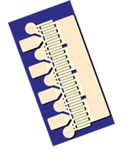
Model TGF2023-2-05 (Fig. 2) is a GaN-on-SiC HEMT designed to provide 25 W output-power from DC to 18 GHz. It is capable of +43-dBm saturated output power at 3 GHz with 78.3% PAE. The model offers 18-dB nominal power gain at 3 GHz in a chip size of 0.82 × 1.44 × 0.10 mm. The GaN-on-SiC HEMT is rated for quiescent current of 100 to 500 mA at drain voltages of +12 to +32 VDC (the recommended drain voltage range is +28 to +32 VDC), and can handle as much as +40 VDC drain voltage and 5 A drain current. It is rated for CW input-power levels as high as +37 dBm.
Model TGF2023-2-10 boasts 50 W output power from DC to 18 GHz, with +47.3-dBm nominal saturated output power at 3 GHz. It achieves maximum PAE of 69.5% with nominal power gain of 19.8 dB at 3 GHz. The power device, which measures 0.82 × 2.48 × 0.10 mm, operates with quiescent current of 200 to 1000 mA at drain voltages of +12 to 32 VDC, with maximum drain voltage rating of +40 VDC and maximum drain current of 10 A.
Finally, the highest-power member of the new GaN-on-SiC HEMT family is model TGF2023-2-20, which is designed for applications from DC to 18 GHz and reaches +50.5 dBm nominal saturated output power at 3 GHz with 70.5% maximum PAE. The nominal power gain at 3 GHz is 19.2 dB. As with the other HEMT devices, it is fabricated with TriQuint’s TQGaN25 production process, developed to optimize microwave power and efficiency at high bias voltages. Measuring just 0.82 × 4.56 × 0.10 mm, this rugged power device is rated for drain voltages of +12 to +32 VDC and quiescent currents of 400 to 2000 mA. The maximum drain voltage is +40 VDC while the maximum drain current is 20 A. The HEMT can handle input-power levels to +43 dBm.
These GaN-on-SiC active devices are fabricated with a proven, stable process and offer relatively high gain and certainly high output-power levels across broad bandwidths through 18 GHz. They are designed for relatively high-bias voltages, but such supplies are readily available in most commercial and military systems, making these devices “plug-and-play” solutions for many applications requiring higher gain and higher power densities.
TriQuint Semiconductor, Inc., 2300 Northeast Brookwood Pkwy., Hillsboro, OR 97124; (972) 994-8465, FAX: (972) 994-8504.
This file type includes high resolution graphics and schematics when applicable.
About the Author
Jack Browne
Technical Contributor
Jack Browne, Technical Contributor, has worked in technical publishing for over 30 years. He managed the content and production of three technical journals while at the American Institute of Physics, including Medical Physics and the Journal of Vacuum Science & Technology. He has been a Publisher and Editor for Penton Media, started the firm’s Wireless Symposium & Exhibition trade show in 1993, and currently serves as Technical Contributor for that company's Microwaves & RF magazine. Browne, who holds a BS in Mathematics from City College of New York and BA degrees in English and Philosophy from Fordham University, is a member of the IEEE.
