Data Converters Drive RF Designs
Data converters are an "end point" on a system block diagram for many RF/microwave designers—the points at which analog signals are converted to digital bits and back again. In recent years, those data converters have gotten faster and boast higher resolution, allowing them to take on a greater portion of receiver and transmitter block diagrams. Some of the leading analog-to-digital converter (ADC) and digital-to-analog-converter (DAC) suppliers made noise with new product introductions at this year’s IEEE International Microwave Symposium (IMS) in Montreal, Canada. Meanwhile, most (if not all) major suppliers sought to improve upon the bandwidths and speeds covered by their products.
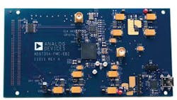
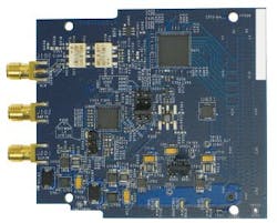
In terms of market dominance, a report from analyst firm Databeans (www.databeans.net) earlier this year noted that Analog Devices (www.analog.com) led the worldwide market with a 48.5% share. At the 2012 IMS,the company introduced a pair of digital transceivers for high-speed applications: the model AD9739A 14-b RF DAC and the model AD9467 16-b ADC. Both can be supplied on a native field-programmable-gate-array (FPGA) mezzanine card (FMC) evaluation board to simplify prototyping efforts.
The model AD9739A DAC (Fig. 1)is a 14-b device that runs to 2.5 GSamples/s and is capable of synthesizing wideband signals from DC through 3 GHz. It is pin- and functionally compatible with the firm’s earlier model AD9739 DAC, except that it does not support synchronization and is designed for use between 1.6 and 2.5 GSamples/s. Elimination of the synchronization circuitry results in some nonideal signal artifacts—such as images and discrete clock spurious products—remaining stationary on the DAC between power-up cycles, making it possible to perform a system calibration.

The AD9739A DAC also incorporates on-chip controllers to simplify system integration. A dual-port, source-synchronous LVDS interface simplifies digital interfaces with existing FGPA/ASIC technology. On-chip controllers are used to manage external and internal clock domain variations over temperature to ensure reliable data transfer from the host to the DAC core. A serial peripheral interface (SPI) is used for device configuration as well as readback of status registers. The DAC is manufactured on a 0.18-μm CMOS process and operates from 1.8 and 3.3 V supplies. It is supplied in a 160-ball chip scale ball grid array.
For lower-frequency chores, model AD9467 (Fig. 2) is a 16-b monolithic intermediate-frequency (IF) ADC which operates at a 250 MSamples/s conversion rate. It is suitable for handling the IF signals of wireless receivers, instrumentation, and test equipment that require a high dynamic range. It requires supplies of 1.8 and 3.3 VDC and a low-voltage differential input clock for full-performance operation. The data outputs are LVDS (ANSI-644) compatible.
The firm also introduced the model 9128 16-b, 12.5-GSamples/s transmit DAC with integrated complex digital modulation functionality and a JESD204A-compatible serial input. The AD9128’s high-speed serial interface greatly simplifies and improves the data connection between the DAC and the FPGA in a typical system implementation, where FPGAs are more often being used in the roles of system processors. But the data bottlenecks into and out of an FPGA have traditionally limited their performance at high sampling rates. The JESD204 high-speed serial interface is scalable and accommodates data rates in the multiple Gb/s range. The DAC provides four lanes of high-speed JESD204A serial links.
The AD9128 DAC includes an on-chip 32-b numerically controlled oscillator (NCO) for flexible placement of the system intermediate frequency (IF), along with the use of complex modulation and gain and offset compensation. A four-wire serial port interface provides for programming and read-back of many of the device’s internal parameters and functions. The DAC supports a wide range of wireless communications standards, including GSM, CDMA2000, and fourth-generation (4G) Long Term Evolution (LTE) systems.
For speed, the MAX5881 DAC from Maxim Integrated Products (www.maxim-ic.com) is optimized for direct synthesis of multichannel downstream quadrature amplitude modulation (QAM) signals in cable-modem termination systems (CMTS) and edge QAM devices. Operating at sampling rates to 4.3 GSamples/s, it can directly synthesize multiple channels in the 50 to 1000 MHz cable downstream band for data-over-cable service interface specification (DOCSIS®) use.
The current-steering DAC includes four 12-b multiplexed low-voltage-differential-signaling (LVDS) input ports, each operating to 1075 MHz in double-data-rate (DDR) or quad-data-rate (QDR) mode. It accepts clock signals at one-half the DAC update rate, since data conversion is triggered on both rising and falling clock edges. The input data rate is one-quarter the DAC update rate or one-half the clock rate. The MAX5881 is capable of operating at clocks rate to 2.15 GHz, resulting in a DAC update rate of 4.3 GSamples/s. An LVDS data clock output simplifies interfaces to FPGAs or application-specific integrated circuits (ASICs). The MAX5881 operates on supplies of +3.3 and +1.8 VDC and consumes only 1.3 W power at 4.3 GSamples/s.
The firm also announced their model MAX19693 12-b DAC for direct-digital synthesis of wideband signals. The 4-GSamples/s converter can be used for synthesis of wideband signals in the frequency range from DC to nearly 2 GHz. The 4-GSamples/s update rate enables digital synthesis of signals with more than 1.5-GHz bandwidth.
The DAC includes four 12-b multiplexed low-voltage differential signaling (LVDS) input ports, each operating to 1 GHz in double data rate (DDR) or quad data rate (QDR) mode. The DAC accepts a clock at one-half the DAC update rate, since conversion is triggered on both rising and falling clock edges. The input data rate is one-quarter the DAC update rate.
The complement of data converters once offered by National Semiconductor (www.national.com) were acquired by Texas Instruments (TI; www.ti.com) in the latter half of 2011, so all of those components are now available from the latter company. As a sampling, the 12-b direct RF sampling ADCs from TI can capture signals to and beyond 2.7 GHz at 12-b resolution and at sampling rates to 3.6 GSamples/s. Using this device, a single direct-sampling ADC can replace a good part of the architecture of a traditional IF or zero-IF (ZIF) radio signal path based on RF mixers, local oscillators (LOs), amplifiers, and filters. The firm’s ADC12Dxx00RF family of ADCs is available in speed grades ranging from dual-channel 500-MSamples/s devices to single-channel 3.6-GSamples/s devices.
Model ADC12D1800RF is a 12-b, single 3.6 GSamples/s RF sampling ADC for direct use with RF signals to 2.7 GHz and above. It can also be used as a dual 1.8 GSamples/s ADC. It includes a flexible LVDS interface with multiple SPI programmable options.
Earlier this year, Fujitsu Laboratories Ltd. (www.fujitsu.com) announced an ADC design that was 50% smaller and consumed 50% less power than conventional ADCs. By using digital control techniques that no longer require the use of a switch of generation of a reference level, Fujitsu developed an ADC with 6-b resolution and conversion rate of 1 Gsamples/s in a die area of only 0.04 mm2, with power consumption of only 9.9 mW.
Meanwhile Tektronix Component Solutions (www.component-solutions.tek.com) offers data converter modules suitable for measurement applications, such as the TADC-1000 module which can digitize one channel at 12.5 GSamples/s or two channels, each at 6.25 GSamples/s. The 8-b ADC module includes parallel LVDS outputs for simple interfacing to FPGAs. The module can stream at continuous rates to 100 GSamples/s and included on-board calibration capability to achieve the highest effective number of bits (ENOB). It exhibits a spurious-free dynamic range (SFDR) of −47 dBc through 5 GHz. The converter module is based on a Tektronix ADC implemented in a silicon-germanium (SiGe) semiconductor process from IBM (www.ibm.com).
The ISLA214S40 is a series of low-power 14-b ADCs fabricated on a standard CMOS process from Intersil (www.intersil.com). Based on the firm’s Femtocharge™ technology, the ADCs can operate at sampling rates to 500 MSamples/s. The converters offer a highly configurable, JESD204B-compliant, high-speed serial output link with data rates to 4.375 Gb/s per lane and multiple packing modes. The link can be configured to use two or three lanes to transmit conversion data.
About the Author
Jack Browne
Technical Contributor
Jack Browne, Technical Contributor, has worked in technical publishing for over 30 years. He managed the content and production of three technical journals while at the American Institute of Physics, including Medical Physics and the Journal of Vacuum Science & Technology. He has been a Publisher and Editor for Penton Media, started the firm’s Wireless Symposium & Exhibition trade show in 1993, and currently serves as Technical Contributor for that company's Microwaves & RF magazine. Browne, who holds a BS in Mathematics from City College of New York and BA degrees in English and Philosophy from Fordham University, is a member of the IEEE.
